Renewable Power Application based Switched Boost
advertisement

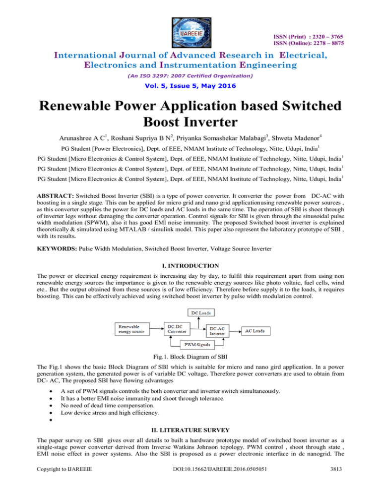
ISSN (Print) : 2320 – 3765 ISSN (Online): 2278 – 8875 International Journal of Advanced Research in Electrical, Electronics and Instrumentation Engineering (An ISO 3297: 2007 Certified Organization) Vol. 5, Issue 5, May 2016 Renewable Power Application based Switched Boost Inverter Arunashree A C1, Roshani Supriya B N2, Priyanka Somashekar Malabagi3, Shweta Madenor4 PG Student [Power Electronics], Dept. of EEE, NMAM Institute of Technology, Nitte, Udupi, India1 PG Student [Micro Electronics & Control System], Dept. of EEE, NMAM Institute of Technology, Nitte, Udupi, India1 PG Student [Micro Electronics & Control System], Dept. of EEE, NMAM Institute of Technology, Nitte, Udupi, India1 PG Student [Micro Electronics & Control System], Dept. of EEE, NMAM Institute of Technology, Nitte, Udupi, India1 ABSTRACT: Switched Boost Inverter (SBI) is a type of power converter. It converter the power from DC-AC with boosting in a single stage. This can be applied for micro grid and nano grid applicationusing renewable power sources , as this converter supplies the power for DC loads and AC loads in the same time. The operation of SBI is shoot through of inverter legs without damaging the converter operation. Control signals for SBI is given through the sinusoidal pulse width modulation (SPWM), also it has good EMI noise immunity. The proposed Switched boost inverter is explained theoretically & simulated using MTALAB / simulink model. This paper also represent the laboratory prototype of SBI , with its results. KEYWORDS: Pulse Width Modulation, Switched Boost Inverter, Voltage Source Inverter I. INTRODUCTION The power or electrical energy requirement is increasing day by day, to fulfil this requirement apart from using non renewable energy sources the importance is given to the renewable energy sources like photo voltaic, fuel cells, wind etc.. But the output obtained from these sources is of low efficiency. Therefore before supply it to the loads, it requires boosting. This can be effectively achieved using switched boost inverter by pulse width modulation control. Fig.1. Block Diagram of SBI The Fig.1 shows the basic Block Diagram of SBI which is suitable for micro and nano gird application. In a power generation system, the generated power is of variable DC voltage. Therefore power converters are used to obtain from DC- AC, The proposed SBI have flowing advantages A set of PWM signals controls the both converter and inverter switch simultaneously. It has a better EMI noise immunity and shoot through tolerance. No need of dead time compensation. Low device stress and high efficiency. II. LITERATURE SURVEY The paper survey on SBI gives over all details to built a hardware prototype model of switched boost inverter as a single-stage power converter derived from Inverse Watkins Johnson topology. PWM control , shoot through state , EMI noise effect in power systems. Also the SBI is proposed as a power electronic interface in dc nanogrid. The Copyright to IJAREEIE DOI:10.15662/IJAREEIE.2016.0505051 3813 ISSN (Print) : 2320 – 3765 ISSN (Online): 2278 – 8875 International Journal of Advanced Research in Electrical, Electronics and Instrumentation Engineering (An ISO 3297: 2007 Certified Organization) Vol. 5, Issue 5, May 2016 structure and advantages of the proposed SBI-based nanogrid are discussed in detail. The dq synchronousreferenceframe-based controller for SBI, which regulates DC and AC bus voltages of the nanogrid to their respective reference values under steady state as well as under dynamic load variation. The control system of SBI is implemented experimentally validated using a 0.5-kW laboratory prototype of the SBI supplying both DC and AC loads at same time III. PROPOSED TOPOLOGY The SBI is a power converter of single input dual output. Fig. 2 shows the proposed SBI circuit diagram. It is a buckboost type DC-AC converter. The SBI is placed in between voltage source and voltage source Inverter Bridge. The main components are an electronic switch (S), inductor (L), high speed diode (D) , voltage source inverter bridge(VSI) and a capacitor (C), DC voltage source (Vg). A low pass filter (Lf and Cf) to filter the inverter bridge output. The operation of SBI under steady state is explained as below Mode 1: During the positive half cycle, the time D·Ts, the Fig.3(a) shows the equivalent circuit diagram of SBI the switch (S) is ON as Vc > Vg the diodes Da & Db are reverse biased . Vc = Vsn1 Inverter is in shoot through state and it assumed to be shorted, capacitor charges the inductor through switch (S) therefore inductor current increases linearly. During this interval inductor current is equal to capacitor discharging current. Fig.2. Circuit Diagram of SBI Mode 2: During the time (1-D) ·Ts the negative of cycle equivalent circuit of SBI is as shown in Fig.3(b) the switch (S) is OFF . The inverter is in non shoot through state & is represented by current source Ii . The Da and Db diodes are forward biased Vsn1= Vi (Inverter input voltage). Energy stored in inductor is discharges through the diodes therefore voltage source and inductor both are supplying power to the inverter. The capacitor charges through diode Da. Fig. 3(a) SBI Circuit diagram during positive half cycle D·Ts and 3(b) During negative half cycle the period (1-D·Ts) Under steady state, . Copyright to IJAREEIE + − . (1 − ) = 0 => = ( ( ) ) DOI:10.15662/IJAREEIE.2016.0505051 (1) 3814 ISSN (Print) : 2320 – 3765 ISSN (Online): 2278 – 8875 International Journal of Advanced Research in Electrical, Electronics and Instrumentation Engineering (An ISO 3297: 2007 Certified Organization) Vol. 5, Issue 5, May 2016 IV.PWM CONTROL FOR SBI In this paper the proposed SBI is controlled by sine-triangle Pulse Width Modulation (SPWM) signals with unipolar voltage switching. Fig.4. shows the schematic circuit of PWM. Vm(t) is a sinusoidal modulation signal of amplitude M.Vp, Vp is a magnitude of constant signal Vst and “ M is a modulation index” fs is a switching frequency of Vtri(t) should be chosen much greater than the frequency fo of sinusoidal signal Vm(t), To maintain the Vm(t) nearly constant in any switching cycle . Sinusoidal, triangular and a constant is compared with each other as shown in Fig.4.from that will get the gate Signals Gs1,Gs2 ,Sa and Sb. these signals are further gone through the NAND operation, to generate the shoot through and non shoot through signals for SBI. The purpose of inserting the signals Sa and Sb is to obtain the shoot through interval DTs in the gate signals of the inverter bridge. Fig.4. Schematic Control Circuit of PWM This PWM control strategy says that “shoot-through state of SBI will have no effect on the harmonic spectrum of its output voltage Fig.10. shows the Harmonic Spectrum of VAB provided that the sum modulation index and duty should be less than unity [5] ” The logical expression used to obtain the required PWM control signals for switches is given as follows: G = G +S G = G +S G = G +S G = S +S G = G +S (2) (3) (4) (5) (6) M+D ≤ 1 (7) V. MODELING OF SBI USING MATLAB / SIMULINK MODEL Modeling of PWM control signals Simulink model of PWM control signal is as shown in fig.5 Also the parameter values used in PWM modeling is as shown in Table.1.The relationship between the shoot through duty ratio D and VST is (D should not be more than 0.5 because the conversion ratio Vg/Vc is very high at D=0.5) D = 1- (8) Table.1. The parameter values used in PWM model Copyright to IJAREEIE Parameter Amplitude Frequency Vm(t) 0.5 50 Hz VST 0.6 50Hz Vtri(t) 1 10KHz DOI:10.15662/IJAREEIE.2016.0505051 3815 ISSN (Print) : 2320 – 3765 ISSN (Online): 2278 – 8875 International Journal of Advanced Research in Electrical, Electronics and Instrumentation Engineering (An ISO 3297: 2007 Certified Organization) Vol. 5, Issue 5, May 2016 Shoot through width (Vsn1= Vc, Vi =0) must lesser than width of zero interval (VAB = 0). Therefore, () DT < T − max (9) D< 1−M M = max V > ( ) (10) (11) ·V (12) Fig.5. Model of PWM Control Signal A generated PWM signal is as shown in Fig.6. are given to the respective gates of converter and inverter bridge. Fig.6.Generated PWM Signals. Copyright to IJAREEIE DOI:10.15662/IJAREEIE.2016.0505051 3816 ISSN (Print) : 2320 – 3765 ISSN (Online): 2278 – 8875 International Journal of Advanced Research in Electrical, Electronics and Instrumentation Engineering (An ISO 3297: 2007 Certified Organization) Vol. 5, Issue 5, May 2016 Table 2: Parameters values used in simulation Parameters Values Input voltage(Vg) 12V Fundamental frequency(fo) 100 F Switching frequency (fs) 10kHz Shoot through duty ratio (D) 0.4 Inductor (L) 5.6mH Modulation index(M) 0.5 Capacitor(C) 100 F Lf 4.6Mh Cf 100 F R 100 Proposed SBI circuit is implemented using MATLAB/SIMULINK model by using parameter values as given in Table1, Fig.7. shows the simulation model of SBI. Fig.7.Simulation Model of Proposed SBI Table.3 SBI output values Copyright to IJAREEIE Parameters MATLAB/Simulink Experimental Vg 12V 12V Vo 20 V 18V DOI:10.15662/IJAREEIE.2016.0505051 3817 ISSN (Print) : 2320 – 3765 ISSN (Online): 2278 – 8875 International Journal of Advanced Research in Electrical, Electronics and Instrumentation Engineering (An ISO 3297: 2007 Certified Organization) Vol. 5, Issue 5, May 2016 Table.3 shows the results obtained from proposed SBI model. Also Fig.8 shows the inverter output voltage VAB and Fig.9 shows the AC output voltage Vo Therefore from this power converter, boosting and conversion of DC –AC in a single stage is achieved effectively Fig.8.Inverter output voltage Fig.9.Output Voltage ( Vo) of SBI Fig.10. Harmonic Spectrum of VAB VI.EXPERIMENTAL SET UP AND RESULTS Table.4. Components used in experiment Components MOSFET Diode Pic controller Gate driver Copyright to IJAREEIE Manufacturer IRF540N U1560 Pic6F877A TLP250 DOI:10.15662/IJAREEIE.2016.0505051 3818 ISSN (Print) : 2320 – 3765 ISSN (Online): 2278 – 8875 International Journal of Advanced Research in Electrical, Electronics and Instrumentation Engineering (An ISO 3297: 2007 Certified Organization) Vol. 5, Issue 5, May 2016 Table.4. shows the list of components used in set up of laboratory prototype of SBI is as shown in fig 10. Here step down transformers supply power to the low side and high side MOSFET separately also used as input voltage source Vg by using bridge rectifier BR1005. Main SBI circuit and controller is isolated through gate driver TLP250. Piccontroller generate the low frequency pulses for inverter bridge, TL494 to generate the high frequency PWM signal for gate Gs. The results obtained from experimental set up is as shown in below Figs Fig 11 Gate signals for Inverter Bridge Fig 12 Gate signals of switch S Fig13 SBI DC output voltage Fig 13 SBI output voltage VAB VII.CONCLUSION This paper gives a theoretical analysis of SBI. The PWM control signals are generated using a MATLAB/SIMULINK. The generated PWM signals verified by applying these signal to a simulation model of SBI and we get the boosted and converted AC output voltage. The inverter Output voltage and its harmonic spectrum, proves that the “shoot-through state of SBI will have no effect on the harmonic spectrum of its output voltage provided that the sum modulation index and duty should be less than unity”. Experimental results are verified by comparing SBI simulink model and laboratory prototype results. This can be implemented effectively in micro grid application by using renewable power sources. REFERENCES [1] [2] [3] [4] [5] [6] Ravindranath, Avinash Joshi,Saurabh Upadhayay.“ A Switched-Boost Topology for Renewable Power Application,”IPCE , pp 758-762,2010 Y. Z peng. “Z-source Inverter ,” IEEE transaction , pp 504-510, 2004. N. Mohan, Undeland, W. T Robbins “Power Electronics Converters” New York: Wiley (1995). D. M. Vilathgamuwa, Y. S. Lai, G. T. Chua and Y. Li. “ Pulse Width Modulation of Z source inverter.” IEEE Trans. on Power Electronics, pp 1346-1355.2004 Ravindranath Adda, Avinash Joshi, Santanu K. Mishra and Olive Ray. “A PWM Control Strategy for Switched Boost Inverter.” Dept. of Electrical Engineering IEEE Trans. on power electronics, pp 5593-5602,2010 Santanu K. Mishra and Avinash Joshi. “Synchronous Reference Frame Based Control of SBI for Standalone DC Nano grid Applications.” IEEE Trans. on power electronics, pp 1219-1233,2011 Copyright to IJAREEIE DOI:10.15662/IJAREEIE.2016.0505051 3819


