Stop-band and band-pass characteristics in coplanar waveguides
advertisement

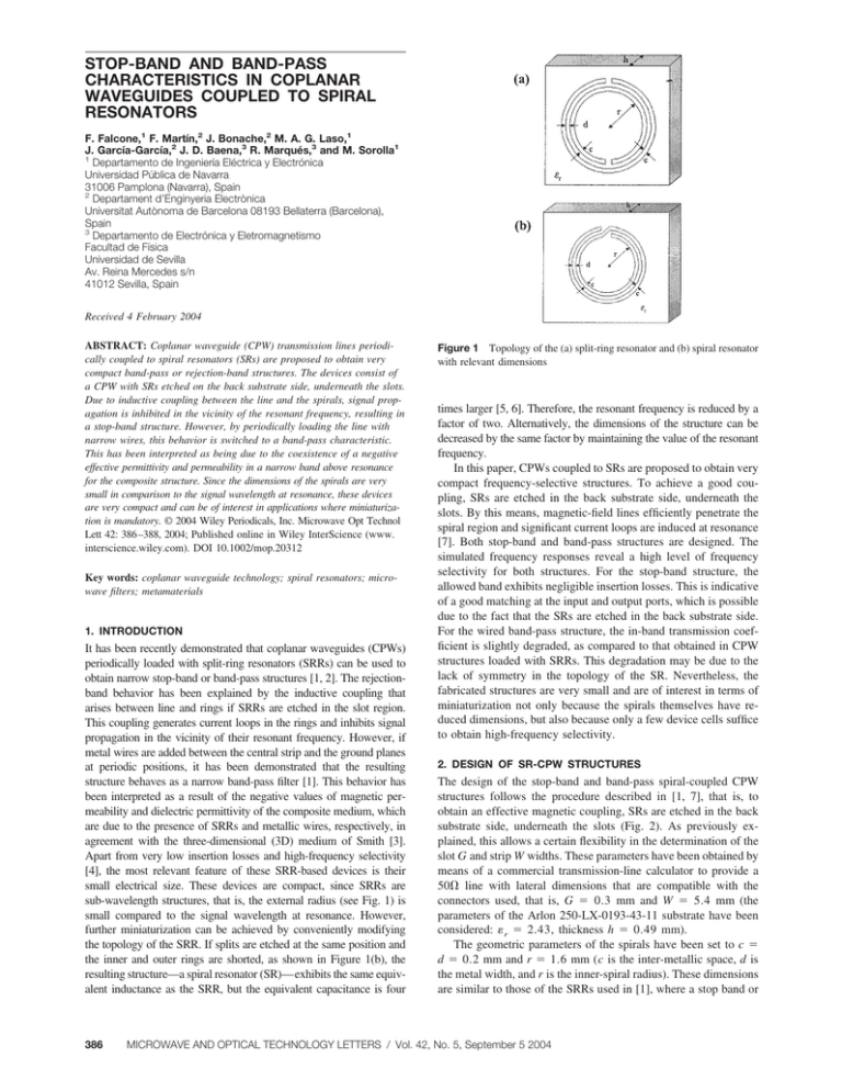
STOP-BAND AND BAND-PASS CHARACTERISTICS IN COPLANAR WAVEGUIDES COUPLED TO SPIRAL RESONATORS F. Falcone,1 F. Martı́n,2 J. Bonache,2 M. A. G. Laso,1 J. Garcı́a-Garcı́a,2 J. D. Baena,3 R. Marqués,3 and M. Sorolla1 1 Departamento de Ingenierı́a Eléctrica y Electrónica Universidad Pública de Navarra 31006 Pamplona (Navarra), Spain 2 Departament d’Enginyeria Electrònica Universitat Autònoma de Barcelona 08193 Bellaterra (Barcelona), Spain 3 Departamento de Electrónica y Eletromagnetismo Facultad de Fı́sica Universidad de Sevilla Av. Reina Mercedes s/n 41012 Sevilla, Spain Received 4 February 2004 ABSTRACT: Coplanar waveguide (CPW) transmission lines periodically coupled to spiral resonators (SRs) are proposed to obtain very compact band-pass or rejection-band structures. The devices consist of a CPW with SRs etched on the back substrate side, underneath the slots. Due to inductive coupling between the line and the spirals, signal propagation is inhibited in the vicinity of the resonant frequency, resulting in a stop-band structure. However, by periodically loading the line with narrow wires, this behavior is switched to a band-pass characteristic. This has been interpreted as being due to the coexistence of a negative effective permittivity and permeability in a narrow band above resonance for the composite structure. Since the dimensions of the spirals are very small in comparison to the signal wavelength at resonance, these devices are very compact and can be of interest in applications where miniaturization is mandatory. © 2004 Wiley Periodicals, Inc. Microwave Opt Technol Lett 42: 386–388, 2004; Published online in Wiley InterScience (www. interscience.wiley.com). DOI 10.1002/mop.20312 Key words: coplanar waveguide technology; spiral resonators; microwave filters; metamaterials 1. INTRODUCTION It has been recently demonstrated that coplanar waveguides (CPWs) periodically loaded with split-ring resonators (SRRs) can be used to obtain narrow stop-band or band-pass structures [1, 2]. The rejectionband behavior has been explained by the inductive coupling that arises between line and rings if SRRs are etched in the slot region. This coupling generates current loops in the rings and inhibits signal propagation in the vicinity of their resonant frequency. However, if metal wires are added between the central strip and the ground planes at periodic positions, it has been demonstrated that the resulting structure behaves as a narrow band-pass filter [1]. This behavior has been interpreted as a result of the negative values of magnetic permeability and dielectric permittivity of the composite medium, which are due to the presence of SRRs and metallic wires, respectively, in agreement with the three-dimensional (3D) medium of Smith [3]. Apart from very low insertion losses and high-frequency selectivity [4], the most relevant feature of these SRR-based devices is their small electrical size. These devices are compact, since SRRs are sub-wavelength structures, that is, the external radius (see Fig. 1) is small compared to the signal wavelength at resonance. However, further miniaturization can be achieved by conveniently modifying the topology of the SRR. If splits are etched at the same position and the inner and outer rings are shorted, as shown in Figure 1(b), the resulting structure—a spiral resonator (SR)— exhibits the same equivalent inductance as the SRR, but the equivalent capacitance is four 386 Figure 1 Topology of the (a) split-ring resonator and (b) spiral resonator with relevant dimensions times larger [5, 6]. Therefore, the resonant frequency is reduced by a factor of two. Alternatively, the dimensions of the structure can be decreased by the same factor by maintaining the value of the resonant frequency. In this paper, CPWs coupled to SRs are proposed to obtain very compact frequency-selective structures. To achieve a good coupling, SRs are etched in the back substrate side, underneath the slots. By this means, magnetic-field lines efficiently penetrate the spiral region and significant current loops are induced at resonance [7]. Both stop-band and band-pass structures are designed. The simulated frequency responses reveal a high level of frequency selectivity for both structures. For the stop-band structure, the allowed band exhibits negligible insertion losses. This is indicative of a good matching at the input and output ports, which is possible due to the fact that the SRs are etched in the back substrate side. For the wired band-pass structure, the in-band transmission coefficient is slightly degraded, as compared to that obtained in CPW structures loaded with SRRs. This degradation may be due to the lack of symmetry in the topology of the SR. Nevertheless, the fabricated structures are very small and are of interest in terms of miniaturization not only because the spirals themselves have reduced dimensions, but also because only a few device cells suffice to obtain high-frequency selectivity. 2. DESIGN OF SR-CPW STRUCTURES The design of the stop-band and band-pass spiral-coupled CPW structures follows the procedure described in [1, 7], that is, to obtain an effective magnetic coupling, SRs are etched in the back substrate side, underneath the slots (Fig. 2). As previously explained, this allows a certain flexibility in the determination of the slot G and strip W widths. These parameters have been obtained by means of a commercial transmission-line calculator to provide a 50⍀ line with lateral dimensions that are compatible with the connectors used, that is, G ⫽ 0.3 mm and W ⫽ 5.4 mm (the parameters of the Arlon 250-LX-0193-43-11 substrate have been considered: r ⫽ 2.43, thickness h ⫽ 0.49 mm). The geometric parameters of the spirals have been set to c ⫽ d ⫽ 0.2 mm and r ⫽ 1.6 mm (c is the inter-metallic space, d is the metal width, and r is the inner-spiral radius). These dimensions are similar to those of the SRRs used in [1], where a stop band or MICROWAVE AND OPTICAL TECHNOLOGY LETTERS / Vol. 42, No. 5, September 5 2004 Figure 2 Layouts for the CPW structures coupled to SRs (a) without and (b) with shunt connected metal wires a band pass in the vicinity of 7.7 GHz was measured in the fabricated structures (r is slightly higher for the SR). Therefore, in the devices designed in this work, where SRRs are substituted by spirals, the frequencies of interest are expected to be in the vicinity of 3.5 GHz. Finally, the distance between adjacent SRs has been set to l ⫽ 5 mm. This parameter allows certain gap/band width control, although within certain restrictive limits (a procedure to enhance gap/band width in stop/pass band structures has been presented elsewhere [2, 4] and is beyond the scope of this paper). The layouts for the designed implementations (stop-band and band-pass structures) are depicted in Figure 2. The unique difference between both designs is the presence of signal-to-ground shorts, (width 0.2 mm) in the band-pass structure. Figure 3 (a) Simulated and (b) measured frequency responses for the device of Fig. 2(a). Insertion and return losses are depicted by bold and thin lines, respectively The simulated frequency response for the circuit of Figure 2(b) indicates the presence of a narrow allowed band above the resonant frequency of spirals (Fig. 4). This is an expected result explained by the presence of shunt-connected metal wires, which cause the structure to behave like a one-dimensional (1D) microwave plasma, with a negative effective permittivity up to the plasma frequency [1]. Since the spiral-coupled CPW structure emulates a composite medium with negative-valued permeability in a narrow band above spiral resonance, the combined wire/spiral CPW structure allows signal propagation at those frequencies where negative permittivity and permeability simultaneously coexist, and behaves as a narrowband left- 3. RESULTS The frequency response for the devices shown in Figure 2 has been obtained by means of the electromagnetic simulation tool CST Microwave Studio. The results, depicted in Figures 3 and 4, confirm the presence of a rejection/pass band in the vicinity of the resonant frequency of the SRs. For the structure of Figure 2(a), a narrow stop band appears centered at 3.5 GHz with rejection levels near 20 dB and very sharp transition bands. This structure has been fabricated by means of a standard photo/mask etching technique and the frequency response has been measured by means of an Agilent 8722ES vector network analyzer. Experimental data (Fig. 3) are in good agreement with the simulations. It is worth mentioning the low level of losses in the pass band, which is below 1 dB in the first allowed band and does not exceed 3 dB in the upper pass band, at least up to a frequency of 8 GHz. This aspect is very important with regard to the use of SRs to reject undesired frequency bands or frequency parasitics in functional devices, since this can be achieved by preserving overall circuit performance. Figure 4 Simulated frequency response for the device shown in Fig. 2(b). Insertion and return losses are depicted by bold and thin lines, respectively MICROWAVE AND OPTICAL TECHNOLOGY LETTERS / Vol. 42, No. 5, September 5 2004 387 handed material. However, in comparison to the SRR/wire structure presented in [1], in-band insertion losses are not as good. This is thought to be due to the lack of symmetry of the spiral resonators, which may give rise to some kind of undesired interaction between wires and spirals, resulting in band-pass degradation. In the SRR/wire CPW medium, this interaction was precluded by properly aligning wires and SRRs [4]. Nevertheless, the main relevant characteristics of SRs are their dimensions. Although combined with metal wires in CPWs, they cannot compete with SRRs in terms of circuit performance; it is very clear that, when coupled to a CPW to achieve a rejection-band structure, they are very promising. Similar performance to that obtained with SRRs coupled to a CPW has been demonstrated, but with the added advantage of lower dimensions for the same resonant frequency. 4. CONCLUSION In conclusion, it has been demonstrated that spiral resonators can be used as constitutive elements in narrowband CPW stop-band and band-pass structures. In comparison to SRRs, the key advantage of spirals is miniaturization, where dimensions reduced by a factor of two are expected for the same resonant frequency, or, alternatively, the resonant frequency is reduced by the same factor if the dimensions are maintained, as has been shown in the paper. It has been demonstrated that, when coupled to CPWs, spirals are able to provide rejection levels in the vicinity of resonance comparable to those obtained with SRRs. In band-pass structures, where metal wires are added between the signal and ground, good frequency selectivity has been obtained, but with higher in-band insertion losses than those obtained with CPW and SRRs. Nevertheless, for the first time the potentiality of spiral resonators in the fabrication of metamaterial-based structures (including negative and left handed) in CPW technology has been pointed out. The results of this work are patent pending. ACKNOWLEDGMENTS This work has been supported by DGI and CICYT under project contracts BFM2001-2001, TIC2002-04528-C02-01, TIC2001-3163, and PROFIT-070000-2003-933. REFERENCES 1. F. Martı́n, F. Falcone, J. Bonache, R. Marqués, and M. Sorolla, A new split ring resonator based left handed coplanar waveguide, Appl Phys Lett 83 (2003), 4652– 4654. 2. F. Martı́n, F. Falcone, J. Bonache, T. Lopetegi, R. Marqués, and M. Sorolla, Miniaturized CPW stop band filters based on multiple tuned split ring resonators, IEEE Microwave Wireless Compon Lett (to appear). 3. D.R. Smith, W.J. Padilla, D.C. Vier, S.C. Nemat-Nasser, and S. Schultz, Composite medium with simultaneously negative permeability and permittivity, Phys Rev Lett 84 (2000), 4184 – 4187. 4. F. Falcone, F. Martı́n, J. Bonache, R. Marqués, T. Lopetegi, and Mario Sorolla, Left-handed coplanar waveguide band-pass filters based on bi-layer split-ring resonators, IEEE Microwave Wireless Compon Lett (to appear). 5. R. Marqués, J.D. Baena, J. Martel, F. Medina, F. Falcone, M. Sorolla, and F. Martı́n, Novel small resonant electromagnetic particles for metamaterial and filter design, Int Conf Electromagn Adv Applic ICEAA, Torino, Italy, 2003. 6. J.D. Baena, R. Marqués, and F. Medina, Artificial magnetic metamaterial design by using spiral resonators, Phys Rev B (to appear). 7. F. Falcone, F. Martin, J. Bonache, R. Marqués, and M. Sorolla, Coplanar waveguide structures loaded with split ring resonators, Microwave Opt Technol Lett 40 (2004), 3– 6. © 2004 Wiley Periodicals, Inc. 388 MICROSTRIPLINE FED DUALFREQUENCY DIELECTRIC RESONATOR ANTENNA Y. Sung, C. S. Ahn, and Y.-S. Kim Dept. of Radio Sciences Engineering Korea University Seoul 136-701, Korea Received 13 February 2004 ABSTRACT: In this paper, a dielectric resonator antenna for dual-frequency operation is proposed. The proposed antenna is excited by dual 50⍀ microstriplines and printed in a single metal layer, and therefore is easily constructed. In this design, the operating frequency is mainly controlled by the offset in the position. The return loss, radiation patterns, and antenna gain are measured and discussed. © 2004 Wiley Periodicals, Inc. Microwave Opt Technol Lett 42: 388–390, 2004; Published online in Wiley InterScience (www.interscience.wiley.com). DOI 10.1002/mop. 20313 Key words: dielectric resonator antennas; microstripline-fed antenna; dual-frequency antennas INTRODUCTION In recent years, most antennas for satellite and wireless communications have been made of metal parts. At millimeter-wave frequencies, however, the metallic losses tend to increase drastically with higher operating frequency, especially at the edges of the strip conductors. To reduce the conduction losses, the conductor antennas need to be replaced by some kind of dielectric antenna [1]. The dielectric resonator antenna (DRA) has several advantageous features such as small size, low cost, light weight, no surface wave, and ease of excitation [2, 3]. However, one bottleneck in the development of dielectric resonator antennas is the considerable narrow bandwidth, as compared to that of ordinary microwave antennas. For this reason, dual-frequency operation is an important subject in antenna design and many such designs are known [4]. Dual-frequency antennas exhibit a dual-resonant behavior in a single radiating structure; hence, they may provide convenience in terms of space and cost. Unlike a microstrip patch antenna, little information on the dual-frequency DRA is available in the literature thus far. This is probably due to the relative complexity of the feeding network and inflexibility of the DR shape. In this paper, the DRA fed by microstripline excitation [5] is experimentally investigated to determine its broad region in a variety of resonant frequencies ([5] does not contain such an investigation). Dual-frequency operation can easily be obtained by dual microstriplines located along the centerline of the DR. Therefore, this antenna can be manufactured by a simple procedure. Details of the experimental results are presented and analyzed. ANTENNA CONFIGURATION The physical geometry of the dual-feed dual-frequency antenna is shown in Figure 1. The ring DRA has inner radius a ⫽ 1 mm, outer radius b ⫽ 3.25 mm, height h ⫽ 2.88 mm, and dielectric constant ra ⫽ 37. The DRA has offsets d x and d y , which denote the distance from the edge of the DRA to the edge of the microstripline [see Fig. 1(b)]. The DRA is mounted on a substrate with a relative dielectric constant of 2.5 and a thickness of 0.635 mm. The width of transmission line w is 1.8 mm, which corresponds to a 50⍀ feedline for the substrate used. The grounded dielectric substrate of size 70 ⫻ 70 mm2 is used. The DRA is fed by a pair of orthogonal feedlines with a different offset. MICROWAVE AND OPTICAL TECHNOLOGY LETTERS / Vol. 42, No. 5, September 5 2004


