Turn-on Snubber circuits: • protect switching device from
advertisement
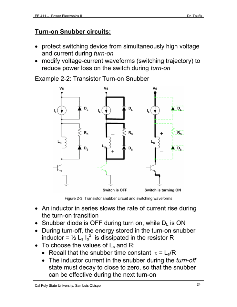
EE 411 – Power Electronics II Dr. Taufik Turn-on Snubber circuits: • protect switching device from simultaneously high voltage and current during turn-on • modify voltage-current waveforms (switching trajectory) to reduce power loss on the switch during turn-on Example 2-2: Transistor Turn-on Snubber Figure 2-3. Transistor snubber circuit and switching waveforms • An inductor in series slows the rate of current rise during the turn-on transition • Snubber diode is OFF during turn on, while DL is ON • During turn-off, the energy stored in the turn-on snubber inductor = ½ Ls Io2 is dissipated in the resistor R • To choose the values of Ls and R: • Recall that the snubber time constant τ = Ls/R • The inductor current in the snubber during the turn-off state must decay to close to zero, so that the snubber can be effective during the next turn-on Cal Poly State University, San Luis Obispo 24 EE 411 – Power Electronics II Dr. Taufik • If say, 3 time constant is necessary for inductor discharge, then: toff state > 3* Ls/R Pspice Simulations: 80 Switching Waveform at Turn-On without Snubber 40 0 17.9980ms V(Q2:c) 17.9990ms 50*IC(Q2) 18.0000ms 18.0010ms 18.0020ms 18.0030ms 18.0010ms 18.0020ms 18.0030ms Time 80 Switching Waveform at Turn-On with Snubber 40 0 17.9980ms V(Q1:c) 17.9990ms 50*IC(Q1) 18.0000ms Time 19.8W Turn-on Losses WITHOUT Snubber 10.0W WITH Snubber 0W 17.99900ms IC(Q1)*V(Q1:c) 18.00000ms IC(Q2)*V(Q2:c) 18.00100ms 18.00200ms 18.00300ms 18.00400ms Time Figure 2-4. Pspice Example to show effect of Snubber Cal Poly State University, San Luis Obispo 25 EE 411 – Power Electronics II Dr. Taufik Energy Recovery Snubber circuits: • With turn-off and turn-on snubbers, the power dissipated in the switching device may be reduced • At the same time, snubbers transfer the power to the snubber resistor which dissipates power loss as heat • Not an energy efficient solution 1. Need to eliminate the use of snubber resistor 2. Need to transfer the stored energy in the snubber to the load or back to the source 3. A method that satisfies (1) and (2) is called the Energy Recovery Snubber circuits 4. Energy Recovery Snubber is also known as Nondissipative snubber Advantages of nondissipative snubber: • Increase operating efficiency • Can be cost effective in high-power equipment Disadvantages • More complex circuit • More components: reliability issue, added cost, weight Example 2-3: Transistor Energy Recovery Snubber Figure 2-5. Transistor Energy Recovery Snubber Circuit Cal Poly State University, San Luis Obispo 26 EE 411 – Power Electronics II Dr. Taufik • When the switch is turning OFF • Ds and Cs act like the turn-off snubber • During turn-off, Cs charges to Vs and delays the voltage rise across the transistor • When the switch is turning ON • Diodes DL and D2 are off • A current path Cs, D1, C1 and Q is formed, and thus charging capacitor C1 • The charge initially stored in Cs is transferred to C1 • At the next turn-off: • C1 discharges through D2 into the load, while Cs charges again Cal Poly State University, San Luis Obispo 27 EE 411 – Power Electronics II Dr. Taufik Example 2-4: Transistor Energy Recovery Snubber Figure 2-6. Another Transistor Energy Recovery Snubber Circuit • Assume initially C2 has been charged to Vs, then when Q1 turns off energy from L1 goes to C2, through path Load-L1C2-CR1 Figure 2-7. Charging C2 Cal Poly State University, San Luis Obispo 28 EE 411 – Power Electronics II Dr. Taufik • When Q1 turns on, then current flows through path C2-Q1CR2-L2 while charging L2 Figure 2-8. Charging L2 • When Q1 turns off again (CR1 turns on again), the energy stored in L2 is now delivered back to C1, hence to back to the input source, through path L2-CR1-C1-CR2 Figure 2-9. Discharging back to C1 Cal Poly State University, San Luis Obispo 29 EE 411 – Power Electronics II Dr. Taufik Other Snubber Circuits: • There are wide varieties of Snubber circuits depending on: • The semiconductor switches used • The purpose of the snubbers (turn-off, turn-on, combined, energy recovery, over-voltage, etc.) • Other useful references for various Snubbers: • Power Electronic Text-Books • Engineering Database such as Applied Science & Technology, Engineering Village 2 • US Patent search engine: patent.womplex.ibm.com/ Other Examples of Snubbers: Rectifier Snubbers • Can reduce voltage transients and EMI Figure 2-10. Rectifier Snubber Circuit [4] • Top snubber is recommended for a high output current • Bottom snubber is recommended for low output currents and/or high-voltage outputs Cal Poly State University, San Luis Obispo 30 EE 411 – Power Electronics II Dr. Taufik Triac Snubbers • For lamp load Figure 2-11. TRIAC Snubber Circuit [4] • For inductive load Figure 2-12. TRIAC Snubber Circuit with Inductive Load [4] • to alleviate di/dt and dv/dt Figure 2-13. TRIAC Snubber Circuit for di/dt and dv/dt [4] Cal Poly State University, San Luis Obispo 31 EE 411 – Power Electronics II Dr. Taufik SCR Snubber Figure 2-14. SCR Snubber Circuit [4] Cal Poly State University, San Luis Obispo 32 EE 411 – Power Electronics II Dr. Taufik MOSFET Snubbers: Figure 2-15. MOSFET Snubber Circuit [4] Cal Poly State University, San Luis Obispo 33 EE 411 – Power Electronics II Dr. Taufik Alternative to Snubbers • So far we have discussed switching technique where the switch in the circuit is required to turn on from significantly high voltage and to turn off from significantly high current • Called the Square-wave switching or Hard-switching • High switching dv/dt and di/dt stresses • Associated with EMI (Electro-Magnetic Interference) problem due to large di/dt and dv/dt noises • Switching losses since the switch absorbs crucial amount of power loss that increases linearly with the switching frequency • Snubber Circuits alleviate switching losses: • Help by shifting the energy loss from the switching devices to the snubber components • Not a good solution since • Do not necessarily suppress total loss, hence may not improve overall converter’s efficiency • Limit the operating switching frequency • since snubbers slow down the rate of rise and fall times • consequently reduce maximum duty cycle • Associated with additional components • Extra cost • More reliability consideration • May increase size and weight • Theoretically, snubbers won’t be needed if • The switch is operated in such a way that the voltage across it and/or the current through it is ZERO at the switching instants or transitions • No auxiliary circuit added to the switch - cost efficient • Switching frequency can be increased, without increasing switching loss and thus total loss • reduce filter requirement and thus converter size and weight in general Cal Poly State University, San Luis Obispo 34 EE 411 – Power Electronics II Dr. Taufik Converter topology which incorporates either ZERO Voltage or ZERO Current switching or both is called: ) The Soft-switching Topology ( • The soft-switching topology can be achieved for example by using resonant circuit • Examples of switching trajectory using Hard-switching, Hard-switching+Snubber, and Soft-switching in Bridge Converter: 1. Switch Mode 2. Switch Mode with Snubbers 3. ZVS/ZCS Switching Figure 2-16. Examples of Switching Trajectories [5] Cal Poly State University, San Luis Obispo 35 EE 411 – Power Electronics II Dr. Taufik Self Assessment Study 1. What are Snubber Circuits? 2. List two uses of Snubber Circuits. 3. Why Snubber Circuits do not always reduce the total loss of converter. 4. How does a turn-off transistor snubber reduce turn-off switching loss? 5. In the turn-off transistor snubber, how do you select the snubber capacitor? 6. How do you select the snubber resistor in the turn-off transistor snubber? 7. What are Energy-recovery Snubbers? 8. List disadvantages of using Snubbers. 9. What is Soft-Switching? 10. What are the advantages of Soft-Switching over the Snubbers? Cal Poly State University, San Luis Obispo 36 EE 411 – Power Electronics II Dr. Taufik Chapter 3: Soft-Switching Review of Resonant Circuits Basic Resonant Circuit Concepts Two types of Basic Resonant Circuit 1. Series-Resonant Circuits • Undamped Series-Resonant Circuit • Series-Resonant Circuit with a Capacitor-Parallel Load 2. Parallel-Resonant Circuits • Undamped Parallel Resonant Circuit Undamped Series-Resonant Circuit L1 1u V1 I 1 C1V 1u 0 2.0 Capacitor Voltage 1.0 0 Inductor Current -1.0 1.980ms 1.982ms V(C1:2) I(L1) 1.984ms 1.986ms 1.988ms 1.990ms 1.992ms 1.994ms 1.996ms 1.998ms 2.000ms Time Figure 3-1. Undamped Series-Resonant Circuit and waveforms with no initial conditions Cal Poly State University, San Luis Obispo 37 EE 411 – Power Electronics II Dr. Taufik Using KVL: Lr di L + vc = Vd dt and Cr dvc = iC = iL dt The solution of these differential equations for Vd − Vc 0 sin ω o t Z0 vc (t ) = Vd − (Vd − Vc 0 ) cosω o t + Z 0 I L 0 sin ω o t where: IL0 = initial condition of the inductor Vc0 = initial condition of the capacitor ωo = angular resonant frequency = 2πf o = 1 iL (t ) = I L 0 cosω o t + (1) (2) [Amps] [Volts] [rad/sec] Lr C r Zo = characteristic impedance = [Ohms] Lr Cr 4 Cases: 1. When no initial conditions (Zero initial conditions) are found in L1 and C1 Vd sin ω o t Z0 vc (t ) = Vd − Vd cos ω o t iL (t ) = See Figure 3-1 for Inductor and Capacitor waveforms 2. When both L1 and C1 posses initial conditions Equations (1) and (2) Cal Poly State University, San Luis Obispo 38 EE 411 – Power Electronics II Dr. Taufik 3.0 Vc(0)=0.5V IL(0)=0.25A Capacitor Voltage 2.0 0 Inductor Current -2.0 1.980ms 1.982ms V(C1:2) I(L1) 1.984ms 1.986ms 1.988ms 1.990ms 1.992ms 1.994ms 1.996ms 1.998ms 2.000ms Time Figure 3-2. Undamped Series-Resonant Circuit and with initial conditions on both L and C 3. When only C1 has the initial condition Vd − Vc 0 sin ω o t Z0 vc (t ) = Vd − (Vd − Vc 0 ) cos ω o t iL (t ) = 3.0 Vc(0)=0.5V IL(0)=0A Capacitor Voltage 2.0 0 Inductor Current -2.0 1.980ms 1.982ms V(C1:2) I(L1) 1.984ms 1.986ms 1.988ms 1.990ms 1.992ms 1.994ms 1.996ms 1.998ms 2.000ms Time Figure 3-3. Undamped Series-Resonant Circuit and with initial condition on C only 4. When only L1 has the initial condition iL (t ) = I L 0 cos ωot + Cal Poly State University, San Luis Obispo Vd sin ω0t Z0 39 EE 411 – Power Electronics II Dr. Taufik vc (t ) = Vd − Vd cos ω0t + Z 0 I L 0 sin ωot 3.0 Vc(0)=0V IL(0)=0.25A Capacitor Voltage 2.0 0 Inductor Current -2.0 1.980ms 1.982ms V(C1:2) I(L1) 1.984ms 1.986ms 1.988ms 1.990ms 1.992ms 1.994ms 1.996ms 1.998ms 2.000ms Time Figure 3-4. Undamped Series-Resonant Circuit and with initial condition on L only Cal Poly State University, San Luis Obispo 40
