Improved Effective Capacitance Computations for Use in Logic and
advertisement
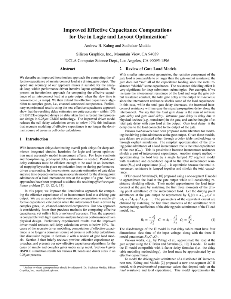
Improved Effective Capacitance Computations for Use in Logic and Layout Optimization Andrew B. Kahng and Sudhakar Muddu Silicon Graphics, Inc., Mountain View, CA 94039 UCLA Computer Science Dept., Los Angeles, CA 90095-1596 Abstract We describe an improved iterationless approach for computing the effective capacitance of an interconnect load at a driving gate output. The speed and accuracy of our approach makes it suitable for the analysis loop within performance-driven iterative layout optimization. We present an iterationless approach for computing the effective capacitance of an interconnect load at a gate output when the slew time is non-zero (i.e., a ramp). We then extend this effective capacitance algorithm to complex gates, i.e., channel-connected components. Preliminary experimental results using the new effective capacitance approach show that the resulting delay estimates are quite accurate – within 15% of HSPICE-computed delays on data taken from a recent microprocessor design in 0.25µm CMOS technology. The improved driver model reduces the cell delay calculation errors to below 10%; this indicates that accurate modeling of effective capacitance is no longer the dominant source of errors in cell delay calculation. 1 Introduction With interconnect delays dominating overall path delays for deep submicron integrated circuits, heuristics for logic and layout optimization must accurately model interconnect effects. For logic synthesis and floorplanning, pre-layout delay estimation is needed. Post-layout delay estimates must be efficient enough to be used in an incremental mapping/layout/in-place optimization loop or during performancedriven area routing. In these contexts, accurate estimation of gate delay and rise time depends on having an accurate model for the driving point admittance of a load interconnect tree at the output of a gate. Various approaches have been proposed to address the resulting effective capacitance problem [7, 15, 12, 6, 13]. In this paper, we improve the iterationless approach for computing the effective capacitance of an interconnect load at a driving gate output. We use an accurate driver resistance computation to enable effective capacitance calculation when the interconnect load is driven by complex gates, i.e., channel-connected components. Our new approach is considerably faster than previous methods for computing effective capacitance, yet suffers little or no loss of accuracy. Thus, the approach is compatible with tight synthesis-analysis loops in performance-driven physical design. Preliminary experimental results that the improved driver model reduces cell delay calculation errors to below 10%. Because of the accurate driver modeling, computation of effective capacitance is no longer a dominant source of errors in cell delay calculation. Our discussion begins in Section 2 with a review of gate load models. Section 3 then briefly reviews previous effective capacitance approaches, and presents our new effective capacitance algorithms for the cases of simple and complex gates under ramp input. Section 4 gives HSPICE simulation results for various RC loads and driver sizes in an 0.25µm process. Author to whom correspondence should be addressed: Dr. Sudhakar Muddu, Silicon Graphics, Inc., muddu@mti.sgi.com. 2 Review of Gate Load Models With smaller interconnect geometries, the resistive component of the gate load is comparable to or larger than the gate output resistance: the gate does not “see” all of the capacitance loading since the metal resistance “shields” some capacitance. The resistance shielding effect is very significant for deep-submicron technologies. For example, if we increase the interconnect resistance of the load and keep the gate output resistance constant, the total gate delay at the output will decrease since the interconnect resistance shields some of the load capacitance. In this case, while the total gate delay decreases, the increased interconnect resistance will increase the signal propagation delay along the interconnect. We say that the total gate delay is the sum of intrinsic gate delay and gate load delay. Intrinsic gate delay is delay due to physical devices (e.g., transistors) in the gate, and can be thought of as total gate delay with zero load at the output. Gate load delay is the delay due to the load connected to the output of the gate. Various load models have been proposed in the literature for modeling the driving point admittance at the gate output. Given these models, gate delays are estimated either through a delay table methodology or through explicit simulation. The simplest approximation of the driving point admittance of a load interconnect tree is the total capacitance of the tree (Ctot ). This is pessimistic because interconnect resistance shields a part of interconnect capacitance. Another simple method – approximating the load tree by a single lumped RC segment model with resistance and capacitance equal to the total interconnect resistance (Rtot ) and capacitance (Ctot ) – is optimistic because the total interconnect resistance is lumped together and shields the total capacitance. O’Brien and Savarino [9, 10] proposed using a one-segment Π model to approximate the load at the gate output while still considering resistance shielding effects. Their model approximates the load interconnect at the gate by matching the first three moments of the driving point admittance of the interconnect load. Let the driving point i admittance at the gate output be represented by YL (s) = ∑∞ i=1 Ai s = sA1 + s2 A2 + s3 A3 + : : :. The parameters of the equivalent circuit are obtained by matching the first three moments of the admittance with corresponding coefficients of the driving point admittance of the Π load model, i.e., R1 = ,A23 A32 C1 = A1 , A22 A2 C2 = 2 A3 A3 : (1) The disadvantage of the Π model is that delay tables must have four dimensions: slew time of the input voltage, along with the three Π model parameters R1 ; C1 ; C2 . Various works, e.g., by Pillage et al., approximate the load at the gate output using the O’Brien and Savarino [9, 10] Π model. To make the Π model compatible with k-factor delay formulas (i.e., the delay table modeling methodology), the load must be approximated by an effective capacitance. To model the driving point admittance of a distributed RC interconnect tree, Kahng and Muddu [2] proposed a new one-segment RC Π model, with predetermined parameter values that depend only on the total resistance and total capacitance. This model approximates the entire interconnect tree by an equivalent open-ended RC line whose resistance and capacitance are equal to the total interconnect resistance and capacitance. The distributed nature of the load interconnect is still considered in calculating model parameters, but the approach is more efficient since the moments of the driving point admittance are obtained without recursive tree traversal. The admittance of an open-ended RC line can be obtained from the 2-port parameters as [2] tanh(θ) Z0 2 2 3 , s2 Rtot3Ctot + s3 2Rtot15Ctot + p where the propagation constant θ = R sC , and the characteristic Y (s) = q impedance Z0 = = sCtot ::: tot Rtot sCtot . tot The first three moments of the driving point admittance are A1 = Ctot ; A2 = , tot3 tot ; A3 = in Equation (1) yields Π model parameters R C2 R1 = 12Rtot ; 25 C1 = 2 3 2Rtot Ctot 15 . Substituting Ctot 5Ctot ; and C2 = 6 6 (2) Last, when segmented models are used, each interconnect line is represented by multiple RC or RLC segments. The admittance is recursively computed using the admittance expression for a single RLY segment. The admittance at node i is represented as an infinite series using the admittance moments as Yi (s) = sY1;i + s2Y2;i + : : : + skYk;i + : : : with Yk;i being the coefficients of sk is the kth moment of the admittance of subtree T (i). Ri i Li function allows the effective capacitance to be characterized over the full range of parameter values. Pileggi and coauthors propose an effective capacitance calculation that approximates the output waveform for single stage gates by using a two piece output waveform [15, 12]. This approach calculates an effective capacitance by equating (i) the current at the gate output with driving-point admittance as the load, and (ii) the current at the gate output with a single effective capacitor as the load. It is difficult to obtain a single effective capacitance that will exactly match the actual load in terms of current at the gate output, at all times t. Hence, average currents for both models are equated over some period of time, say, until the gate output voltage reaches the 50% threshold. The approach provides accurate results for computing cell delays. In general, however, previous effective capacitance approaches require costly iterations (e.g., 5 to 10 iterations until the method of [15] converges) and moment computations for the entire load (even though the moment computation is linear, three moments of accuracy requires three traversals of the interconnect topology). They also typically involve empirical equations that assume fast input transitions and/or require extensive characterization effort. We now propose two new and simple, yet accurate, techniques for effective capacitance calculation. We model the load at the gate output with a simple open-ended RC Π model, which eliminates any need for moment computations at the gate output. We also model the gate with a Thevenin equivalent circuit to compute the closed-form equation for the voltage response at the gate output. The value for effective capacitance can be computed by matching the delay/slew time for the Π model response with that of the single capacitance model. We now give details of the effective capacitance computation for the ramp input configuration of the driver model. j A Gate Vin Y B Tree Load VB i Ci Yj A B = Y1; j + Ci Yk;i = Yk; j , Ri k,1 k,2 ∑ Yl iYk,l j , Li ∑ Yl iYk,1,l j , RiCiYk,1 i l =1 ,LiCiYk,2 i ; ; ; for k 2 l =1 ; ; BΠ Beff For the single segment from node i to node j in Figure 1, the kth admittance coefficient at node i is computed according to Observation 1: The admittance at node i in Figure 1 is computed recursively in terms of admittance at node j as [KM96f]: Y1;i B V Figure 1: A single RLC segment between nodes i and j. R1 = 12/25 Rtot V A ; 3 New Methods for Computing Effective Capacitance The previous work of McCormick [7] obtains the effective capacitance as a function of total capacitance (Ctot ), a step input capacitance which depends on the gate output slew rate, and the Elmore delay of the load. The step input capacitance is chosen to approximate the load admittance such that the output voltage waveform of the cell passes through the endpoints of some critical output voltage range (e.g., 0% and 75% ) at identical times. In [13] the effective capacitance is derived as a function of four parameters (output slew and three Π model parameters) in such a way that these parameters can be reduced to two normalized parameters. Normalizing the parameters of the effective capacitance RS VS C eff VS RS C = 1/6 Ctot 1 C = 5/6 Ctot 2 Figure 2: A Thevenin equivalent model of ramp input source, and a driver resistance for the gate. The load at the gate output is modeled in two different ways: (i) using an effective capacitance model, or (ii) using a higher-order model such as a Π model. 3.1 Effective Capacitance Under Ramp Input We model the gate with an equivalent circuit consisting of a ramp input source (vS (t )) and a linear source resistance (RS ), as shown in Figure (2). We propose to use the open-ended Π model for the RC (RLC) network at the output of a gate to estimate the driving point admittance. (Note that the proposed algorithms are independent of the RC load model used for computing the admittance.) Under these conditions, we compute the gate output response analytically using the source resistance RD with ramp input and with the load modeled as a Π model. The response at the gate output B in transform domain is given by VX (s) = Vin (s) (1 + sR1C2 ) 1 + s(RDC1 + RDC2 + R1C2 ) + s2 RD R1C1C2 V0 (1 , e,sTR ) 1 TR s2 = + , RD (C1s+ C2 ) (1 + s1 R1C2 ) 1 , (1 + s2 R1C2 ) 1 b2 s21 (s1 , s2 ) (s , s1 ) b2 s22 (s1 , s2 ) (s , s2 ) pb ,4b= RD (C1 + C2 ) + R1C2 where b1 ,b1 2 1 2 2b2 Input Slew (ps) 100 100 100 100 100 200 200 200 # ; b2 = RD R1C1C2 ; and s1;2 = . Depending on the sign of b21 , 4b2 , the poles of the transfer function can be either real or complex; the time-domain response is computed separately for each case. Substituting for the coefficients b1 and b2 into the condition, we obtain b21 , 4b2 = R2D (C1 + C2 )2 + R21C22 + 2RD R1C2 (C2 , C1 ) = R2D (C1 + C2 )2 + R21C22 + 2RD R1C2 ( 2A22 , A1 A3 ) (3) A3 from which we see that the load admittance parameters should satisfy , A1 A3 ) 0 for the poles to be real. For most practical cases the value of C2 is greater than C1 ; this is also true for the open-ended RC Π model. Hence, we study the case of real poles only, with the voltage at gate output B being " (1 + s1 R1C2 ) s t (1 + s2 R1C2 ) s t V0 t , RD (C1 + C2 ) + e1 , e2 TR b2 s21 (s1 , s2 ) b2 s22 (s1 , s2 ) = rd p (ohm-µm) 717 6336 9018 9900 10293 1045 9515 10514 rdn (ohm-µm) 259 2283 3319 3687 3836 350 3620 3922 Table 1: Device parameters for an 0.25 µm process. (2A2 2 vB (t ) Load Cap. (pf) 0.05 0.5 1.0 1.5 2.0 0.05 1.0 2.0 where rdn and rd p are resistances for a 1µm device, and Wn , Wp are the device widths in microns. Typical values for rdn and rd p for 0:25 µm technology are given in Table 3.1.1 Finally, the effective capacitance is computed in the range between step input capacitance Cstep and total load capacitance Ctot . This is because: (i) when the gate response (or slew rate) under no load is fast, the gate will not see all the load capacitance, and (ii) when the inverter response is slow, then the gate will end up charging all the load capacitance. The range between Cramp and Ctot is enforced by computing (i) the load delay DLD of the gate with Ctot as load, and (ii) # the slew rate DNL of the gate under a no-load condition, then setting Ce f f for t TR = Cramp + (Ctot , Cramp ) 1 + D 1 LD =DNL (8) " V0 (1 + s1 R1C2 )(1 , e,TR s1 ) s1 t TR + e TR b2 s21 (s1 , s2 ) = , (1 + s2 R1C2 )(1 e,TR s2 ) s2 t e b2 s22 (s1 s2 ) , , Algorithm Template 1: Given the following information for a cell: # the characterized output delay table for the cell (4) Perform these steps for effective capacitance computation: for t > TR We use the above response to compute the slew time (or delay with respect to input signal) at any user specified threshold voltage Π is the slew time at the gate output for 50% (e.g. 50%). Assume Tout threshold voltage. If we model the load at the gate output with a single effective capacitance Cramp (we refer to this capacitance as Cramp because of the ramp input source model) then the slew time is given by Tslew = k2 RDCramp . The constant k2 associated with the given threshold voltage vth is obtained by calculating the time-domain response for a simple RC circuit driven by a ramp input source: k2 = = ln ln 1 R 1 + RvDthCTtot RDCtot TR ! Tslew ,R C D tot 1 RD Ctot =TR (e (1 , , t > TR (5) Equating the output slew of the Π model with the slew of a single capacitance Tslew , the single effective capacitance Cramp is computed as Cramp = Π Tout k2 RS (6) We model the gate output resistance as a linear resistance RD , i.e., RD = = rdn Wn rd p Wp for NMOS for PMOS 1. Compute Π model parameters using either Equation (1) or Equation (2) Π by solving for the voltage response at the cell out2. Compute Tout put per Equation (4) Π and R using Equation (6) 3. Compute Cramp from Tout D 4. Use the characterized cell delay table and obtain the delay DLD with Ctot as load and the delay DNL with no load 5. Compute Ce f f using Equation (8) for t TR ! 1) for vth ) the Π model parameters (R1 ; C1 ; C2) (7) As discussed in [2], we believe that our effective capacitance approach gives good delay estimates at threshold voltages between 30% and 60% of supply. However, the tail end of the response for our effective capacitance model can deviate significantly from the actual response [2]. Furthermore, the proposed methods provide accurate estimation of delay estimates, but do not provide accurate output waveforms that may be needed to derive the output waveforms of downstream gates. 3.2 Effective Capacitance for Complex Gates Computing an accurate driver resistance RD is quite difficult for complex gate structures, e.g., channel-connected components. When many transistors are connected in series the total pull-down (NMOS) and pull-up (PMOS) resistance is different from the value obtained by adding individual resistance values. This is due to the change in source voltage 1 Note that the parameters in the Table are obtained using drawn dimensions of the transistors. Actual dimensions of transistor widths and interconnect length/width/spacing are a 64% shrink of drawn dimensions. (The 0:25 µm process refers to actual dimensions.) of intermediate transistors due to non-zero voltage on the intermediate node capacitors, and due to variation in threshold voltage due to source-bulk voltage differences. A straightforward approach for modifying our proposed effective capacitance algorithm to handle complex gates is to start with an initial value of RD and iterate until we converge on correct values for both RD and Ce f f . Such an approach is computationally expensive, and hence we seek an iterationless approach for effective capacitance calculation. In this section, we develop a method for computing driver resistance accurately by evaluting the effective driver strength and considering body effects. To first order, the CMOS device driver strength without consideration of body effects is proportional to WL , where L is channel length and W is the width of the device. We propose to model the channelconnected components by computing the effective driver strength and then multiplying by a body effect coefficient. We have performed fits to detailed simulation data in order to characterize the body effect coefficients for various types of configurations for a given process. The effective drive strength for pull-down and pull-up chains is WNe f f = Kpd [ WPe f f = Kpu [ 1 Ln ] L1 W1 + ::: + Wn 1 Ln ] L1 W1 + ::: + Wn experimental configuration consists of two inverters connected in series. We apply a ramp input with slew time 400ps to the first inverter. The load at the second inverter is an RC tree of varying topology. The size of the first inverter is fixed at Wp =Wn = 100=50 µm. HSPICE delays are computed by simulating the chain of inverters with different second inverter sizes and different load RC trees. We use a static timing tool, within which we have implemented our effective capacitance approach, to compute the delays. Table 3 compares delay estimates for an INV gate using Algorithm Template 1. Table 4 compares delay estimates for a NAND2 gate, again using the effective driver resistance computation in Algorithm Template 1. We see that with the new effective capacitance approach, delay estimates are consistently within 15% of HSPICE-computed delays. INV Size (Wp =Wn )µm 24/12 100/50 100/50 80/40 80/40 200/100 HSPICE Delay (ps) 130 80 115 130 140 55 Estimated Delay (ps) 110 90 125 120 160 65 Total Parasitics R/C 260 Ω / 0.50pF 260 Ω / 0.50pF 710 Ω / 1.40pF 150 Ω / 0.40pF 300 Ω / 0.80pF 1000 Ω / 1.40pF (9) Table 3: Comparison of HSPICE-computed delays and estimated delays output by our in-house timing tool. The timing tool uses the Ce f f where Kpd and Kpu are the body effect coefficients for pull-down (NMOS) approach described above to compute load at the INV output. and pull-up (PMOS) chain of transistors, respectively. Table 3.2 shows the characterization of these body effect coefficients as a function of the number of transistors in the chain. We use these body effect coefficients as indicated in the above equation to compute effective driver strengths. # Transistors Kpd Kpd 1 1.0 1.0 2 1.43 1.60 3 1.80 1.95 4 1.85 2.00 5 1.90 2.10 Table 2: Body effect coefficients for one, two, three, four, and five transistors for both pull-down and pull-up chains. These parameters are obtained for an 0.25 µm CMOS process. NAND2 Size (Wp ; Wn )µm 100,100 100,100 80,80 200,200 HSPICE Delay (ps) 94 129 147 63 Estimated Delay (ps) 103 142 159 70 Total Parasitics R/C 260 Ω / 0.50pF 710 Ω / 1.40pF 150 Ω / 0.40pF 1000 Ω / 1.40pF Table 4: Comparison of HSPICE-computed delays and estimated delays output by our in-house timing tool. The timing tool uses the Ce f f approach described above to compute load at the NAND2 output. Now the driver resistance RD can be expressed as RD = = rdn WNe f f rd p WPe f f for NMOS for PMOS 5 Conclusions (10) where rd p and rdn are resistances for a 1µm device (see Table 1). As described above, we model the gate with an equivalent circuit consisting of a ramp input voltage source vS (t ) and the above expression for driver resistance RD . The response at the gate output when we model the load with an effective capacitance is given by Equation (4). The output slew time from this response can be expressed as k3 RDCe f f , with the constant k3 associated with the given threshold voltage vth being very similar to k2 in Equation (5). The effective capacitance can be computed by following the steps of Algorithm Template 1. 4 Experimental Results We now present a preliminary set of experimental results. Our experiments use the latest 0.25um CMOS process parameters (corresponding to a recent high-end microprocessor design project) to model our gates and interconnects. We use standard CMOS inverters of various sizes to determine the accuracy of our effective capacitance computation. The We have proposed a novel iterationless approach for effective capacitance computation, both in the step input and ramp input regimes. Our new approach is faster than previous methods for computing effective capacitance, with HSPICE simulations confirming that little or no loss of accuracy is incurred. We believe that our technique will be valuable within a tight synthesis-analysis loop, e.g., for performance-driven layout optimization. The improved driver model reduces the cell delay calculation errors to between 5% and 10% (notably for complex gates); with this improvement, modeling of the RC load or the effective capacitance is no longer the dominant source of error in the cell delay calculation. Our recent work has embedded this calculation in a production performance verification flow for high-end microprocessor design. REFERENCES [1] W. C. Elmore, “The Transient Response of Damped Linear Networks with Particular Regard to Wideband Amplifiers”, Journal of Applied Physics 19, Jan. 1948, pp. 55-63. [2] A. B. Kahng and S. Muddu, “Efficient Gate Delay Modeling for [3] [4] [5] [6] [7] [8] [9] [10] [11] [12] [13] [14] [15] Large Interconnect Loads”, Proc. IEEE Multi-Chip Module Conf., Feb. 1996 (Submitted to IEEE Trans. on CAD). A. B. Kahng and S. Muddu,’ “Accurate Analytical Delay Models for VLSI Interconnects”, IEEE Intl. Symposium on Circuits and Systems, Atlanta, May 1996. A. B. Kahng, K. Masuko, and S. Muddu, “Analytical Delay Models for VLSI Interconnects Under Ramp Input”, IEEE ICCAD, Nov. 1996. A. B. Kahng and S. Muddu, “A Glossary on Analysis and Modeling of VLSI Interconnections”, Manuscript, February 1996. A. B. Kahng and S. Muddu, “New Efficient Algorithms for Computing Effective Capacitance”, Proc. ACM/IEEE International Symposium on Physical Design, April 1998, pp. 147-151. S. P. McCormick, “Modeling and Simulation of VLSI Interconnections with Moments”, PhD Thesis, MIT, June 1989. J. K. Ousterhout, “A Switch-level Timing Verifier for Digital MOS VLSI”, IEEE Trans. on CAD, July 1985, pp. 336-349. P. R. O’Brien and T. L. Savarino, “Modeling the Driving-Point Characteristic of Resistive Interconnect for Accurate Delay Estimation”, Proc. IEEE ICCAD, 1989, pp. 512-515. P. R. O’Brien and T. L. Savarino, “Efficient On-Chip Delay Estimation for Leaky Models of Multiple-Source Nets”, Proc. IEEE Custom Integrated Circuits Conf., 1990, pp. 9.6.1-9.6.4. L. T. Pillage and R. A. Rohrer, “Asymptotic Waveform Evaluation for Timing Analysis”, IEEE Trans. on CAD 9 (1990), pp. 352-366. J. Qian, S. Pullela, and L. Pillage, “Modeling the “Effective Capacitance” for the RC Interconnect of CMOS gates”, IEEE Trans. on CAD 13 (1994), pp. 1526-1535. R. Macys, S. McCormick, “A New Algorithm for Computing the “Effective Capacitacne” in Deep Sub-micron Circuits”, Proc. IEEE Custom Integrated Circuits Conference, June 1998, pp. 313316. J. Rubinstein, P. Penfield and M. A. Horowitz, “Signal Delay in RC Tree Networks”, IEEE Trans. on CAD 2 (1983), pp. 202-211. C. Ratzlaff, S. Pullela, and L. Pillage, “Modeling the RC Interconnect effects in a Hierarchical Timing Analyzer”, Proc. IEEE Custom Integrated Circuits Conference, May 1992, pp. 15.6.115.6.4.
