IGBT (Insulated Gate Bipolar Transistor)
advertisement
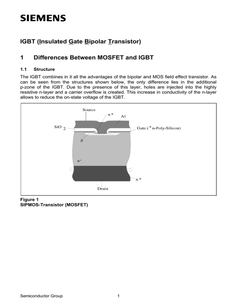
IGBT (Insulated Gate Bipolar Transistor) 1 Differences Between MOSFET and IGBT 1.1 Structure The IGBT combines in it all the advantages of the bipolar and MOS field effect transistor. As can be seen from the structures shown below, the only difference lies in the additional p-zone of the IGBT. Due to the presence of this layer, holes are injected into the highly resistive n-layer and a carrier overflow is created. This increase in conductivity of the n-layer allows to reduce the on-state voltage of the IGBT. Source n+ SiO Al Gate ( 2 p n- n+ Drain Figure 1 SIPMOS-Transistor (MOSFET) Semiconductor Group 1 + n-Poly-Silicon) IGBT Fundamentals Emitter n+ Al SiO Gate ( +n -Poly-Silicon) 2 p n - p Collector Figure 2 IGBT (Insulated Gate Bipolar Transistor) 1.2 Comparison of the Output Characteristics ID [A] 30 20 10 VG 20V 10V 9V 8V 0 0 1 2 3 4 5 VDS[V] Figure 4 Output Characteristics of a MOSFET BUZ 312 (1000 V) Semiconductor Group Figure 3 Output Characteristics of an IGBT BUP 314 (1000 V) 2 IGBT Fundamentals The RDSon of the MOSFET in on-state is mainly influenced by a low doped center region, which is essential for the voltage blocking capability. The additional p-layer of the IGBT causes a carrier overflow in the center region. In spite of the threshold voltage, which is created by the pn-junction at the collector side, a 1000 V-IGBT has an “on-state resistance”, which is reduced by a factor of 5 compared to a MOSFET with similar blocking characterstics and identical chip area. 1.3 The Equivalent Circuit of the IGBT C C GC C R Mod C CE G G C GE E E Figure 5 Equivalent Circuit of the IGBT The equivalent circuit of the IGBT can be depicted quite accurately by a pnp-transistor, where the base current is controlled by a MOS transistor. The conductivity of the resistor on the base branch is increased (modulated) when the IGBT is turned-on. This way, the greater part of the load current is flowing over the base branch. These effects only show for the user by a turn-on delay time and a tail current at turn-off. For this reason, the device can be simply considered as a MOS transistor with the corresponding capacities (see Figure 5). Semiconductor Group 3 IGBT Fundamentals 2 IGBT-Structures Today, two different solutions are known for realizing IGBT that are suitable for existing applications: The PT-structure and the NPT-structure, which has been developed with Siemens. Emitter Emitter n+ n + Al Al + Gate ( n -Poly-Silicon) SiO 2 p p n - n + n -Buffer - p p Collector Collector Figure 7 NPT-IGBT (“homogeneous structure”) Figure 6 PT-IGBT (“epitaxial-structure”) + The PT (punch through) structure shows its characteristic epitaxial layers with an N -doped region (buffer layer) and an N− -region on a p-doped substrate wafer. The carrier life time is minimized by heavy metal diffusion or highly energetic radiation. The base material of the NPT (non punch through) structure is a homogeneous N− -doped wafer. On the backside, a specially formed p-layer is created during wafer processing. It is not necessary to limit the carrier life time. In both cases a typical IGBT cell structure is formed on the front side. Semiconductor Group 4 IGBT Fundamentals 3 Switching Behavior 3.1 Switching Behavior in General IGBTs are mainly used as switches, e.g. in chopper and frequency converter applications. In these applications the adaptation of a (freewheeling) diode is essential, because after switching off the IGBT the current is driven on by the load, which is inductive in most cases. By attaching suitable diodes, this current flow is enabled. When the IGBT is turned on again, the current flown diode (flooded by charge carriers) at first works like a short. The stored charge Qrr has to be removed first for the diode to block voltage. This appears as a surplus current additional to the load current which is called the reverse recovery current of the diode Irr. The maximum of Irr occurs (di/dt = 0) when the sum of the instantaneous voltages across the IGBT and the diode equals the supply voltage (Figure 8). Switching-off the IGBT results in a current change and this makes an overvoltage spike by the current change in the parasitic inductances according to ∆VCE = Lσ × di/dt (Figure 9). Figure 8 Semiconductor Group Figure 9 5 IGBT Fundamentals Miller-Effect The Miller-effect is nothing else than the feedback of the collector-emitter voltage VCE via the gate-collector capacitance CGC on the gate. This means a change of VCE has the same effect as an internal current source into the bias circuit, where the current is given by the expression ig = CGC (VCE) × dVCE/dt. Unfortunately CGC is not constant, but it changes its value with VCE. The strongest change of CGC results at small VCE. This explains that: I C/I C0 V CE/V CE0 V GE/V GE0 During turning-on (starting with: VCE high, VGE zero or negative) with constant gate charging current a linear increase of the gate voltage results. With falling collector-emitter voltage VCE the gate bias current is used for changing the charge of CGC (CGC × dVCE/dt) and the gate voltage remains constant. Later, when the collector-emitter voltage has come down CGC becomes larger as much that also at reduced slope of VCE still all the bias supplied gate current is used up. Only when finally the current needed for charging becomes smaller than the bias supplied current the gate voltage is to rise again (Figure 10). 1,4 1,2 1 V CE 0,8 0,6 0,4 0,2 0 000,0E+0 IC V GE 1,0E-6 2,0E-6 3,0E-6 t [s] Figure 10 Switch-on with Current Commutating from a Freewheeling Circuit Semiconductor Group 6 4,0E-6 IGBT Fundamentals I C/I C0 V CE/V CE0 V GE/V GE0 At turning-off: (starting with: VCE low, VGE positive or greater than threshold voltage Vth) the gate voltage first decreases nearly linearly (at constant gate discharge current). With still low collector-emitter voltage VCE and with only moderate increase there is the strongest change (decrease) of CGC. Decrease of a capacitance at constant charge increases the voltage. As there is a bias source which is drawing current out of the gate, the gate-emitter voltage remains constant. Subsequently VCE increases and most of the gate discharge current is used up for CGC dVCE/dt; the gate voltage further remains constant. The charge over process finally is finished when VCE roughly reaches the operating voltage. Now a further decrease of the gate voltage is possible (Figure 11). 1,2 V CE 1 0,8 V GE IC 0,6 0,4 0,2 0 000,0E+0 1,0E-6 2,0E-6 3,0E-6 4,0E-6 t [s] Figure 11 Turn-off of an Inductive Load into a Freewheeling Circuit By the Miller-effect the gate current during turn-on or turn-off first of all is used for changing the charge of CGC. This is why charging up or down the gate is slowed down. It should be mentioned that CGC-change and VCE-change regulate itself in a way that the available gate current is used up and not more. This means that with a larger gate series resistor all events take a longer time, i.e. turning-on or turning-off last longer. Semiconductor Group 7 IGBT Fundamentals 3.2 Turn-Off Behavior of PT/NPT-IGBT The turn-off behavior of both IGBT-types is different with respect to the temperature dependence. PT-IGBT Figure 12 Strong Increase of Tail-Current With (left 25 °C, right 125 °C) NPT-IGBT Figure 13 The Tail-Current is Nearly Independent of Temperature; the Tail Starting Level is Lower but it Fades Out Slower (left 25 °C, right 125 °C) Semiconductor Group 8 IGBT Fundamentals 3.3 Influence of the Gate-Series-Resistor on the Switching Losses Switching losses have their origin in the overlap of current and voltage waveforms during turn-on and turn-off. They depend on the magnitude of current and voltage. Figure 14 Figure 15 Turn-on speed and by that also turn-on losses can be influenced very easily by the gate series resistor. In turn-off only the current fall-time can be influenced by the gate resistor but, not the tail current. Semiconductor Group 9 IGBT Fundamentals 4 Short-circuit Behavior of the IGBT 4.1 General The negative temperature coefficient of the short-circuit current causes a negative thermal feedback in the device. This is the most important condition for easy paralleling IGBTs. 4.2 Short-circuit Type I This case of short-circuit describes the turn-on of an IGBT during an existing short-circuit in the output circuit (see Figure 16). Figure 16 Schematic of Short-circuit I Figure 17 Output Current/Output Voltage During Short-circuit I In short-circuit mode the IGBT limits the maximum collector current according to its output characteristics. Due to the high voltage while the short-circuit current flows through the IGBT the device has to withstand extremely high power loss. In this case the IGBT has to be turned off in between 5...10 µs. Semiconductor Group 10 IGBT Fundamentals 4.3 Short-circuit Type II Short-circuit type II exists when a short-circuit in the output circuit occurs during the “on phase”, of the IGBT (Figure 18). Limited by the inductivity the current in the output circuit increases. Figure 18 Schematic for Short-circuit Type II Figure 19 Output Current/Output Voltage in Shortcircuit Type II The collector-emitter-voltage increases just when the output current reaches the level corresponding to the gate-emitter-voltage. The increase of the output voltage leads to a strong decrease of the gate-collector-capacity. This causes an internal current which charges up the gate-emitter-capacity (see: Miller-Effect, in chapter 3.1). In some cases the gateemitter-voltage increases far above the allowed level up to 30 V. According to the higher gate-emitter-voltage there is a dynamic short-circuit current peak. It’s value is higher than the stationary short-circuit current depending on the actual gate-voltage. Similar situations appear also in short-circuit type I when there is an inductively limited slow increase of current and the IGBT nearly turns on for a short period of time, which means that the collector-emitter-voltage breaks down to some 10 V. Semiconductor Group 11 IGBT Fundamentals Clamping in Short-circuit Type II Figure 20 Bias Circuit With Actively Clamped Gate Figure 21 Current-/Voltage Response Without Active Clamping Due to the described Miller-Effect the increase of the collector-emitter-voltage causes a current that elevates the gate-voltage if the gate cannot be discharged fast enough. This is especially critical when the IGBT is controlled by a source with a series gate resistor. Therefore it is very important to use a gate clamping in such short-circuit cases. Here active clamping (see Figure 20) is the best method today (if a fast diode is used). Active clamping has advantages compared to Zener clamping between gate and emitter, because the clamped voltage is independent from the spread of the Z-diode voltage and the slope in the output characteristics. In addition when a fast diode is used the charge caused by the MillerEffect can be removed very fast. The dynamic short-circuit current peak can be kept much lower compared to a bias supply without active clamping (Figure 21). Semiconductor Group 12 IGBT Fundamentals 4.4 Safe Operating Area During Short-circuit (SCSOA) normalized shortcut current 25°C 1200V-IGBT-2nd generation 12,00 SOA VGE = 15 V 10,00 VGE = 13 V Isc/Irated 8,00 VGE = 11 V 6,00 4,00 2,00 0,00 0 200 400 600 800 1000 1200 1400 VCE in [V] Figure 22 Safe Operating Area in Short-circuit Case The level of the short-circuit current is determined by the gate voltage of the IGBT. But under normal on-state conditions a low gate-emitter-voltage causes an increase of VCE (sat) and higher forward loss. The resulting short-circuit current for VGE ≤ 15 V is lower than ten times the nominal current. The short-circuit can safely be turned-off in between 10 µs up to the full breakdown voltage of the IGBT. Therefore the protection circuitry can be kept relatively small. But the inductive voltage peak (V = Lσ × di/dt) caused by the set-up must be kept in mind. Semiconductor Group 13

