Microcomputers Digital Signal Processing
advertisement
Microcomputers
Analog-to-Digital and Digital-to-Analog
Conversion
1
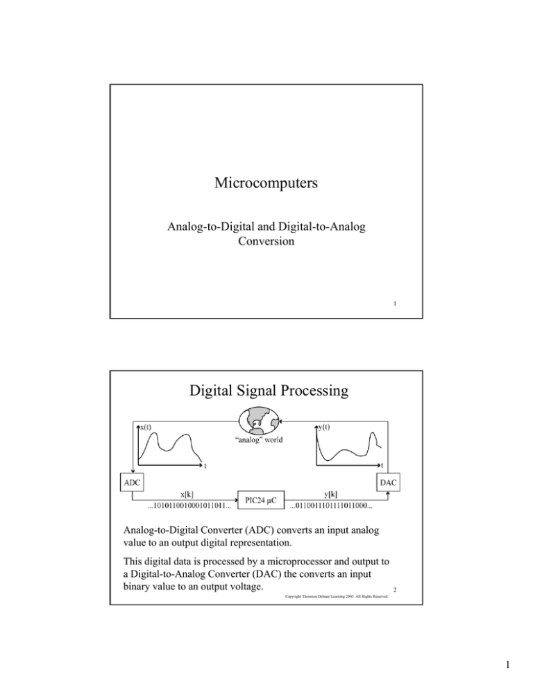
Digital Signal Processing
Analog-to-Digital Converter (ADC) converts an input analog
value to an output digital representation.
This digital data is processed by a microprocessor and output to
a Digital-to-Analog Converter (DAC) the converts an input
binary value to an output voltage.
2
Copyright Thomson/Delmar Learning 2005. All Rights Reserved.
1
Vocabulary
• ADC (Analog-to-Digital Converter) – converts an analog
signal (voltage/current) to a digital value
• DAC (Digital-to-Analog Converter) – converts a digital
value to an analog value (voltage/current)
• Sample period – for ADC, time between each conversion
– Typically, samples are taken at a fixed rate
• Vref (Reference Voltage) – analog signal varies between 0
and Vref, or between +/- Vref
• Resolution – number of bits used for conversion (8 bits, 10
bits, 12 bits, 16 bits, etc).
• Conversion Time – the time it takes for a analog-to-digital
conversion
3
A 1-bit ADC
Vref
analog signal
Vin
R
Vref/2
Vdd
+
Vout=Vdd if Vin > Vref/2
-
Vout=0 if Vin < Vref/2
R
digital signal
comparator
4
2
ADC Resolution
For an N-bit ADC, the smallest input voltage that can be
resolved is 1 LSb, or:
1/2N * (Vref+ - Vref-)
Where Vref+ is the positive reference voltage and
Vref- is the negative reference voltage.
We will use Vref- = 0 V, and refer to Vref+ as simply Vref, so
this simplifies to
1/2N * Vref.
For Vref = 4 V, and N = 4, what is 1 LSb?
1/24 * 4 V = 1/16 * 4 V = 0.25 V.
5
ADC, DAC Equations
ADC: Vin = input voltage, Vref+ = reference voltage, Vref- = 0 V.
Vref
N = number of bits of precision
2N
= output_code
Vin/ Vref *
output_code/ 2N * Vref = Vin
output
code
ADC
Vin
N
1 LSB = Vref/2N
DAC: Vout = output voltage, Vref = reference voltage,
N = number of bits of precision
Vref
Vout/ Vref * 2N = input_code
input_code/ 2N * Vref = Vout
Vout
input
code
DAC
N
1 LSB = Vref/2N
6
3
Sample ADC, DAC Computations
If Vref = 5V, and a 10-bit A/D output code is 0x12A, what is the
ADC input voltage?
Vin = output_code/2N * Vref = (0x12A)/210 * 5 V
= 298/1024 * 5 V = 1.46 V (ADC Vin)
If Vref = 5V, and an 8-bit DAC input code is 0xA9, what is the
DAC output voltage?
Vout = input_code/2N * Vref = (0xA9)/28 * 5 V
= 169/256 * 5 V = 3.3 V (DAC Vout)
If Vref = 4V, and an 8-bit A/D input voltage is 2.35 V, what is the ADC
output code?
output code = Vin/ Vref * 2N = 2.35 V/ 4 V * 28
= .5875 * 256 = 150.4 = 150 = 0x96 (ADC output code)
7
Counter Ramp ADC
Control logic use a counter to apply successive codes
0,1,2,3,4... to DAC (Digital-to-Analog Converter) until DAC
output is greater than Vin. This is SLOW, and have to allocate
the worst case time for each conversion, which is 2N clock
cycles for an N-bit ADC.
Copyright Thomson/Delmar Learning 2005. All Rights Reserved.
8
4
Successive Approximation ADC
Initially set VDAC to ½ Vref, then see if Vin higher or lower
tan VDAC. If > ½ Vref, then next guess is between Vref and ½
Vref, else next guess is between ½ Vref and GND. Do this for
each bit of the ADC. Takes N clock cycles.
9
Copyright Thomson/Delmar Learning 2005. All Rights Reserved.
Successive Approximation Example
Given a 4-bit Successive Approximation ADC, and Vref = 4 V.
Let Vin = 3.14159 V. Clear DAC input to 0b0000.
1. First guess, DAC input = 0b1000 = 8, so Vdac = 8/24* 4 V = 8/16 * 4 V = 2 V.
Vdac (2 V) < Vin (3.14159 V), so guess of ‘1’ for MSb of DAC was correct.
2. Set next bit of DAC to ‘1’, DAC input = 0b1100 = 12, so Vdac = 12/16*4= 3V.
Vdac (3 V) < Vin (3.14159 V), so guess of ‘1’ for bit2 of DAC was correct.
3. Set next bit of DAC to ‘1’, DAC input = 0b1110 = 14, so Vdac = 14/16*4= 3.5V.
Vdac (3.5 V) > Vin (3.14159 V), so guess of ‘1’ for bit1 of DAC was incorrect.
Reset this bit to ‘0’.
4. Set last bit of DAC to ‘1’, DAC input = 0b1101 = 13, so Vdac = 13/16*4 = 3.25V.
Vdac (3.25 V) > Vin (3.14159 V), so guess of ‘1’ for bit0 of DAC was incorrect.
Reset this bit to ‘0’.
Final ADC output code is 0b1100.
Check result: output code = Vin/Vref * 2N = 3.14159/4 * 16 = 12.57 = 12 (truncated).
10
5
A 2-bit Flash ADC
R
Vin
+
A
-
3/4Vref
R
Vin
+
B
-
1/2Vref
R
Vin +
C
-
1/4Vref
A B C
D1 D0
------------0 0 0
0 0
0 0 1
0 1
0 1 1
1 0
1 1 1
1 1
(other codes
don’t cares)
R
Encoding logic
D[1:0]
Fast,
conversion
time is
settling time
of
comparators
and digital
logic.
11
A 3-bit Flash ADC
Copyright Thomson/Delmar Learning 2005. All Rights Reserved.
12
6
ADC Architecture Summary
• Flash ADCs
–
–
–
–
–
Fastest possible conversion time
Requires the most transistors of any architecture
N-bit converter requires 2N-1 comparators.
Commercially available flash converters up to 12 bits.
Conversion done in one clock cycle
• Successive approximation ADCs
– Use only one comparator
– Take one clock cycle per bit
– High precision (16-bit converters are available)
13
Commercial ADCs
• Key timing parameter is conversion time – how
long does it take to produce a digital output once a
conversion is started
• Up to 16-bit ADCs available
• Separated into fast/medium/low speed families
– Serial interfaces common on medium/low speed ADCs
• For high-precision ADCs, challenge is keeping
system noise from affecting conversion
– Assume a 16-bit DAC, and a 4.1V reference, then 1 LSB
= 4.1/216 = 62 V.
14
7
Digital-to-Analog Conversion
For a particular binary code, output a voltage between
0 and Vref
Vref
D[7:0]
Vout
DAC
Assume a DAC that uses an unsigned binary input code,
with 0 < Vout < Vref. Then
D= 0000 0000 Vout = 0V
D= 0000 0001 Vout = Vref(1/256 ) (one LSB)
D = 0000 0010 Vout = Vref(2/256)
...
D = 1111 1111 Vout = Vref(255/256) (full scale)
15
DAC Output Plot
Vout
Output signal
increases in 1 LSB
increments.
4/256 Vref
3/256 Vref
2/256 Vref
1/256 Vref
0
1
2
3
Input code
16
8
Flash DAC
Eliminates
large
capacitive
load at one
node.
Large
capacitive load
N-bit DAC requires 2N resistors!
Copyright Thomson/Delmar Learning 2005. All Rights Reserved.
17
R-2R Ladder DAC
Resistor ladder divides the Vref voltage to a binary weighted
value 4-bit value, with the 4-bits equal to X3 X2 X1 X0
If the switch Xn is connected to Vref, then that bit value is ‘1’, if
the switch Xn is not connected to Vref, then that bit value is ‘0’.
Majority of DACs use this architecture as requires far less
resistors than flash DACs.
Copyright Thomson/Delmar Learning 2005. All Rights Reserved.18
9
Sample DAC Computations
If Vref = 5V, and the 8-bit input code is 0x8A, what is the
DAC output voltage?
input_code/2N * Vref = (0x8A)/28 * 5 V
= 138/256 * 5 V = 2.70 V (Vout)
If Vref = 4V, and the DAC output voltage is 1.25 V, what is
the 8-bit input code?
Vout/ Vref * 2N = 1.25 V/4 V * 28
= 0.3125 * 256 = 80 = 0x50 (input_code)
19
Commercial DACs
• Either voltage or current DACs
– Current DACs require an external operational amplifier
to convert to voltage
• Precision up to 16 bits
• Key timing parameter is settling time - amount of
time it takes to produce a stable output voltage
once the input code has changed
• We will use an 8-bit voltage DAC with a SPI
interface from Maxim semiconductor
20
10
PIC24 ADC
• The PIC24 C has an onboard ADC
– Successive approximation
– 10-bit (default) or 12-bit resolution
– Reference voltage can be Vdd or separate voltage (min
AVSS + 2.7 V)
– Multiple input (more than one input channel)
– Clock source for ADC is either a divided Fosc, or an
internally generated clock. The ADC clock period (Tad)
cannot be less than 76 ns for 10-bit mode, or 118 ns for 12bit mode. The internally generated clock has a period of
~ 250 ns (~ 4 MHz).
21
Block Diagram
Note that different ANx inputs
are mapped to different
‘Channels’, so have to select
both a Channel and an ANx
input.
22
11
Conversion Time
• Total conversion time is sampling time + conversion time
• Sampling looks at the input voltage and uses a storage capacitor to
acquire the input.
– This time is configurable; we will use a conservative 31 Tad periods
which is the maximum for the PIC24HJGP202.
• Conversion time is Number of bits + 31 Tad periods.
• So, for these settings, takes 31 (sampling) + 12 (bits) + 2 = 45 clock
periods.
• Using the internal clock (250 ns), one conversion takes about 11.25 µs
(88.9 kHz).
23
Voltage References
Stability of voltage reference is critical for high precision
conversions.
We will use Vdd as our voltage reference for convenience, but will
be throwing away at least two bits of precision due to Vdd
fluctuations.
Example Commercial voltage reference: 2.048v, 2.5v , 3v, 3.3v,
4.096v, 5v (Maxim 6029). The PIC24 can only used a voltage
reference of either 3.0 V or 3.3 V.
5V
Vdd
4.096v
Vref
Key parameter for a voltage is
stability over temperature operating
range. Need this to be less than ½
of a LSB value.
24
12
Configuring the ADC
void configADC1_ManualCH0(uint16 u16_Ch0PositiveMask,
uint8 u8_autoSampleTime, uint8 u8_Use12bits) {
if (u8_autoSampleTime > 31) u8_autoSampleTime=31;
AD1CON1bits.ADON = 0;
// turn off ADC (changing setting while ADON is
not allowed)
/** Configure the internal ADC **/
AD1CON1 = ADC_CLK_AUTO + ADC_AUTO_SAMPLING_OFF;
if (u8_Use12bits) AD1CON1 |= ADC_12BIT;
AD1CON3 = ADC_CONV_CLK_INTERNAL_RC + (u8_autoSampleTime<<8);
AD1CON2 = ADC_VREF_AVDD_AVSS;
AD1CHS0 = ADC_CH0_NEG_SAMPLEA_VREFN + u16_Ch0PositiveMask;
AD1CON1bits.ADON = 1;
//turn on the ADC
}
Configures for internal ADC clock, uses manual sample start/auto
conversion, and u16_Ch0PositiveMask selects the ANx input from
Channel 0 to convert. Uses AVDD, AVSS as references. Parameter
u8_autoSampleTime sets the number of sample clocks, and
u8_Use12bits determines if 12-bit or 10-bit conversion is done.
25
Starting a Conversion, Getting result:
int16 convertADC1(void) {
SET_SAMP_BIT_AD1();
//start sampling
WAIT_UNTIL_CONVERSION_COMPLETE_AD1(); //wait for conversion to finish
return(ADC1BUF0);
}
In this mode, tell ADC to start sampling, after sampling is
done the ADC conversion is started, and then a status bit
is set when the conversion is finished.
26
13
MAXIM 548 DAC
SPI interface
DAC output
R/2R DAC
Copyright Maxim, from MAX518/517 Datasheet 19-0293
27
Max548A SPI Command Format
First Byte: DAC
command byte
Second Byte: Command data
Command byte to do conversion: 0x09 (0b00001001)
Data is the value to convert.
28
14
Function for doing a DAC conversion:
#define CONFIG_SLAVE_ENABLE() CONFIG_RB3_AS_DIG_OUTPUT()
#define SLAVE_ENABLE()
_LATB3 = 0
#define SLAVE_DISABLE()
_LATB3 = 1
//low true assertion
void writeDAC (uint8 dacval) {
SLAVE_ENABLE();
//assert Chipselect line to DAC
ioMasterSPI1(0b00001001)
//control byte that enables DAC A
ioMasterSPI1(dacval);
//write DAC value
SLAVE_DISABLE();
}
29
Testing the ADC and DAC
The MAX548 is an 8-bit DAC with a SPI port
3.3 V
MAX548
3.3 V
PIC24HJ32GP202
AN0
RB3
SDO1 (RP6)
SCK1 (RP7)
VDD
LDAC#
CS#
DIN
DAC Output
OUTA
GND
SCLK
Potentiometer has three pins - middle pin is the wiper, connect
the end pins to Vdd/Gnd (ordering does not matter).
Read the voltage from the potentiometer via the PIC24 ADC,
write this digital value to the DAC. The DAC output voltage
should match the potentiometer voltage.
30
15
Potentiometer
Vdd
A variable resistor. Tie outer two legs
to Vdd/GND. Voltage on middle leg
will vary between Vdd/GND as
potentiometer is adjusted, changing the
position of the wiper on the resistor.
31
adc_spidac_test.c
void configDAC() {
CONFIG_SLAVE_ENABLE();
SLAVE_DISABLE();
}
int main(void) {
uint16 u16_adcVal;
uint8 u8_dacVal;
float f_adcVal;
float f_dacVal;
//chip select for DAC
//disable the chip select
Use input AN0 on Channel 0
as ADC input
Number of sampling periods,
31 is maximum for
PIC24HJ32GP202
configBasic(HELLO_MSG);
CONFIG_AN0_AS_ANALOG();
configADC1_ManualCH0(ADC_CH0_POS_SAMPLEA_AN0, 31, 1);
configSPI1();
configDAC();
while (1) {
Support function,
configures for manual
sampling, auto conversion
Value of ‘1’ selects 12-bit
mode, ‘0’ selects 10-bit
mode.
32
16
adc_spidac_test.c (cont)
while (1) {
u16_adcVal = convertADC1();
//get ADC value
u8_dacVal = (u16_adcVal>>4) & 0x00FF; //upper 8 bits to DAC value
writeDAC(u8_dacVal);
f_adcVal = u16_adcVal;
f_adcVal = f_adcVal/4096.0 * VREF; //convert to float 0.0 to VREF
f_dacVal = u8_dacVal;
f_dacVal = f_dacVal/256.0 * VREF;
printf("ADC in: %4.3f V (0x%04x), To DAC: %4.3f V (0x%02x) \n",
(double) f_adcVal, u16_adcVal, (double) f_dacVal, u8_dacVal);
DELAY_MS(300);
//delay so that we do not flood the UART.
} //end while(1)
}
u16_adcVal is 12-bit ADC value.
f_adcVal is u16_adcVal converted to a voltage between 0 – 3.3V using a float
data type.
u8_dacVal is the 8-bit value to send to the DAC (upper 8 bits of u16_adcVal ).
f_dacVal is u8_dacVal converted to a voltage between 0 – 3.3V using a float
data type.
33
Program Output
12-bit ADC code
as voltage
12-bit ADC code
8-bit DAC code
8-bit DAC code as
voltage
34
17
What do you have to know?
• Vocabulary
• DAC R/2R architecture
• ADC Flash, Successive approximation
architectures
• PIC24 ADC
– How to configure
– Acquisition, Conversion time
– How to start do conversion, read result
• MAX548A DAC usage
35
18
