LCD Display LCD LCD Control
advertisement

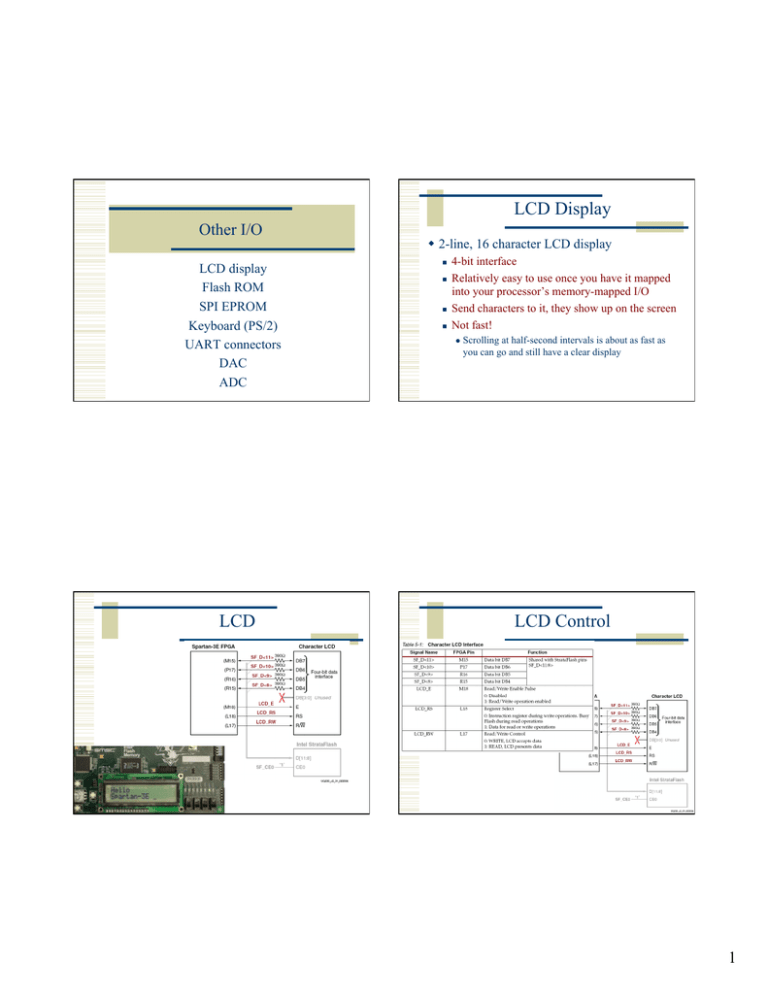
LCD Display Other I/O LCD display Flash ROM SPI EPROM Keyboard (PS/2) UART connectors DAC ADC LCD 2-line, 16 character LCD display 4-bit interface Relatively easy to use once you have it mapped into your processor’s memory-mapped I/O Send characters to it, they show up on the screen Not fast! Scrolling at half-second intervals is about as fast as you can go and still have a clear display LCD Control 1 LCD Control LCD Data Three memory areas inside LCD DD RAM – memory to hold the characters being displayed Two Also CG ROM – Pre-defined character map CG RAM – RAM to hold 8 custom characters 192 5x8 DD RAM DD RAM – memory to hold the characters being displayed Data written to each of these locations is the 8-bit address of a character in the CG ROM/ RAM pre-defined characters bit character/glyphs CG ROM/RAM For example, 8’h53 = S rows of 16 characters to display 24 extras per line that can be scrolled Note the Japanese kana characters… Also, notice the 8 CG RAM locations Addresses 8’h00 to 8’h07 2 CG RAM This example is custom character 0’h03 Note that there are 8 rows in custom character 3 So, it takes 8 writes to make a custom character Row address is incremented automatically… Operation Overview Pick an LCD screen location Write an 8-bit character address to that location Then it shows up on the screen Pick a CG RAM location Write 8 bytes starting at that location Now you can use that new custom character Do it all with just a four-bit interface… Command Set Lots of little nibble writes…. Command Set Commands are sent upper-nibble first 3 Command Set Command Set Commands are sent upper-nibble first Write Timing Memory Mapped I/O So, as a practical matter, the easiest way to deal with the LCD is to map the interface to a memory-mapped location Now you can, under program control, change the values on the data and control wires Your Processor I/O Reg en Writing to the address of the LCD Reg will update its value 4 Initialization Configuration Remember, this display is SLOW compared to 50MHz!!! Using the Display Remember timing! The LCD_E enable pulse must be high for at least 230ns (12 clock cycles at 50MHz) The two nibbles must be separated by 1µs (50 cycles) Two different commands must be separated by 40µs (2000 cycles) But, these are easily done in an assembly language program… (as are the even longer configuration delays) 5 Strata Flash 16 MByte (8 Mword) flash ROM Designed to hold configuration data for the Spartan part But, can be used for general non-volatile data Strata Flash Some data lines are shared with the LCD But, if you don’t read back from the LCD they can both work together Writing to the Strata Flash Tricky! Luckily, there is reference design on the Xilinx web site that implements a Flash programmer Xilinx Flash Project You can use this to load data to your board See class web site in the xilinx examples directory www.eng.utah.edu/~3710/xilinx-docs/examples s3esk_picoblaze_nor_flash_programmer 6 Reading from the Flash Xilinx Example Not as tricky But, the flash has a 75ns access time So, it will take four 50MHz cycles to read data Each cycle is 20ns Set SF_oe and SF_ce active (low) and wait for four cycles (80ns) before grabbing return data… As usual map the flash into your processor’s memory-mapped address space Xilinx Example Read Waveforms 75ns 7 Page Mode Read 75ns SPI Serial Flash 16Mbit – SPI serial protocol Mostly used for Xilinx configuration But, you can use it for data if you want to You can program it using the Impact tool As with all Flash – reading is (relatively) easy, writing is more complex 25ns SPI Serial Flash In this case, reading one byte takes 40 clock ticks… Serial Output Two pins: Clk and Data New data presented at Data pin on every clock Looks like a shift register 8 SPI Serial Flash SPI Serial Flash 32 clocks before data starts coming back (runs up to 75MHz) Then 8 more ticks to get the data (MSB first) PS/2 Keyboard Interface Standard keyboard interface Serial protocol similar to UART, but with its own clock When you press a key, the keyboard sends a “make code” (one, sometimes two, bytes) When you release the key, the keyboard sends a “break code” (two, sometimes three, bytes) Collectively, these are known as “scan codes” 9 PS/2 Keyboard Interface PS/2 Keyboard Interface 20-30 kHz Codes are sent LSB first with Odd parity Note that 11 bits are sent for each code start, 8-data, odd parity, stop Scan Codes (Make Codes) ASCII codes Break codes are the same, but prefixed with 0xF0 for example – Q break code is 0xF0 0x15, is E0 F0 74 10 PS/2 Things to Keep in Mind When you press and hold a key, the make code is sent every 100ms or so If no key is pressed, both clk and data are in their idle state Probably want a PS/2 controller that grabs codes and puts them in a register that can be read by your program (memory mapped I/O) Probably want to set a bit that says “new code” that gets cleared when the code is read UART PS/2 Mouse Whenever the mouse moves it Sends three bytes. Status tells you state of buttons sign of X and Y, and overflow for X and Y UART Basics Two main parts: Connectors Voltage translator You provide the UART circuit! (See 3700 UART for details) 9600 * 8 = 76.8kHz 50MHz/651 = 76.805kHz 11 UART Basics UART Basics 50MHz clock Use rcv-req as a flag to be read by your program? Assert xmt-req by your program to initiate send? Digital to Analog Converter SPI ADC Four-channel 12-bit DAC Serial SPI protocol - up to 50MHz 32-bit data format 12 SPI ADC Other SPI Parts Remember to disable the other SPI devices… Analog Capture Analog to Digital Converter Programmable scaling pre-amplifier 14-bit ADC SPI interface to both of them 13 SPI to Pre-amp SPI to ADC Summary Memory Map All I/O can be mapped into your memory space You have lots of room left over in the addressable space if you use block RAMs only Might need custom FSMs to actually talk to the I/O Control the devices under program control Some memory locations will be data, some will be control Writing or reading these locations will have I/O side effects Remember to consider timing! Think about how your program will interact with I/O Word addresses FFFF 8000 7FFF I/O Switches/LEDs UART Flash ROM? C000 BFFF Glyphs? Block RAM Code/Data 4000 3FFF Code/Data 0000 Top two address bits define regions? Frame buffer? 4k additional words 16k words (32k bytes) 14


