Lecture 2. Transistors
advertisement
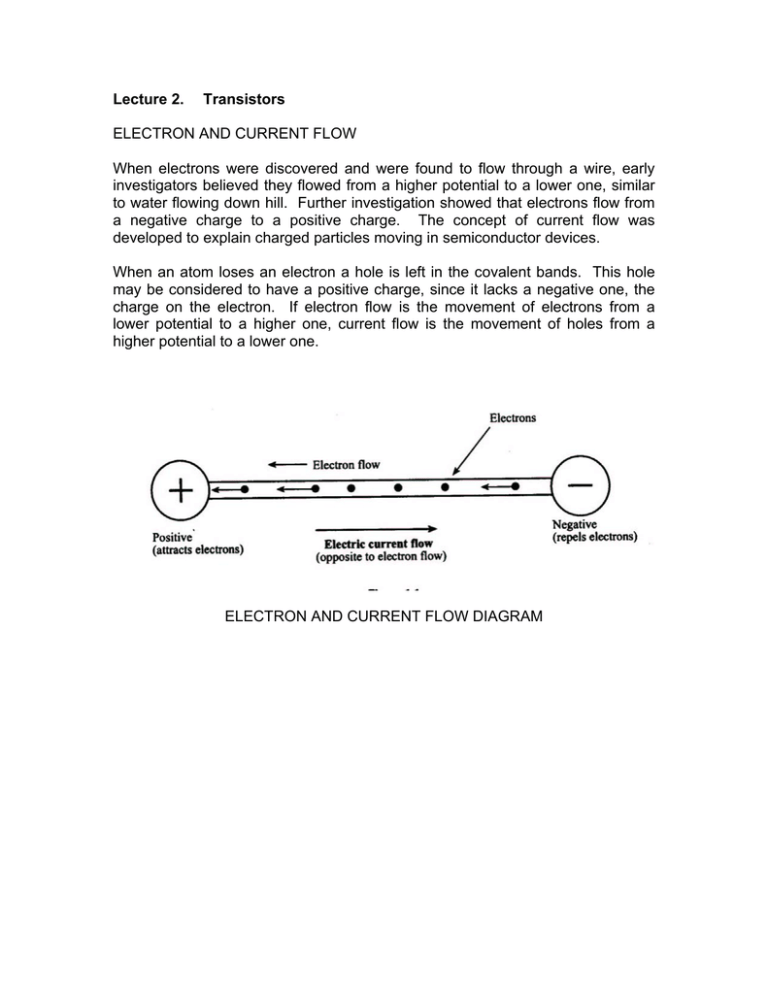
Lecture 2. Transistors ELECTRON AND CURRENT FLOW When electrons were discovered and were found to flow through a wire, early investigators believed they flowed from a higher potential to a lower one, similar to water flowing down hill. Further investigation showed that electrons flow from a negative charge to a positive charge. The concept of current flow was developed to explain charged particles moving in semiconductor devices. When an atom loses an electron a hole is left in the covalent bands. This hole may be considered to have a positive charge, since it lacks a negative one, the charge on the electron. If electron flow is the movement of electrons from a lower potential to a higher one, current flow is the movement of holes from a higher potential to a lower one. ELECTRON AND CURRENT FLOW DIAGRAM DIODE A diode is a two terminal electrical device created by joining two materials together, one having an excess of positive charge carriers, P material, and the other having an excess of negative charge carriers, N material. When the two materials are joined there is a migration of carriers across the junction bond creating a depletion region whereby no charged particles reside. DIFFUSION AT THE PN JUNCTION DEPLETION REGION AFTER DIFFUSION An electric field is created in the depletion region and it has a potential in this area. In order to have current flow through the diode it must be forward biased. Forward biasing makes the depletion region smaller so that it is easier for the current to flow through the device. FORWARD BIAS CIRCUIT Reversing the bias voltage increases the depletion region. REVERSE BIAS CIRCUIT Bipolar Junction Transistor – BJT Here is a picture of the first bipolar junction transistor invented by Bell Laboratories in New Jersey. THE FIRST TRANSISTOR The bipolar junction transistor is basically two diodes connected back to back. The transistors can be made in two different configurations, NPN or PNP. For our study we will use the NPN since it is more common. There are three terminals which need to be connected for the transistor, base, collector, and emitter. The connection between the emitter and base is forward biased and the connection between the collector and base is reversed biased. Pictured below is the biasing for an NPN transistor. NPN TRANSITOR VEE is connected to the base and emitter terminals so that their junction is forward biased. VCC is connected to the collector and base terminals so that their junction is reverse biased. A transistor is a current amplifier and usually the collector current is much larger than the base current, IC >> IB. By controlling the base current, IB, you control the size of the depletion region from the base to the emitter. The narrower the depletion region more electrons flow into the collector. SCHEMATIC SYMBOLS BASIC EQUATIONS IC = β I B , β= β= α 1 −α ,α is usually given in the spec sheet IC IB Gain = output of something input of something There are three different ways to connect a transistor in a circuit: common base common collector common emitter The most widely used configuration is common emitter due to the fact it has power, voltage, and current gain. COMMON EMITTER CHARACTERISTICS The characteristic curves of the common emitter configuration are shown below. The input characteristic curve shows that the base-emitter junction must be biased at least by 500 mV before current will flow. COMMON-EMITTER INPUT CHARACTERISTICS The output curves show typical collector currents dependent upon the base current supplied by the input circuitry and the voltage drop measured across the collector and emitter terminals. COMMON-EMITTER OUTPUT CHARACTERISTICS To make the transistor functional you select resistors that create the base and collector currents, and vCE voltage drop to make it perform to your specifications. If you measure the voltage across the collector and emitter terminals (VCE) and you measure the power supply value (VCC), the collector current (IC) is zero and the transistor is said to be in the cutoff mode. If VCE is zero volts then IC is at the load line maximum and is said to be in saturation mode. TRANSISTOR SWITCH Transistors were first used in telephone circuitry to act as a switch. Control signals were applied to the base of the common-emitter input to either have the transistor in the off condition (the transistor in cutoff mode) or on (the transistor in saturation mode). The first step is to create a load line. For this example Vcc=15V and RL=1,000Ohms. 15 V 1000 ohms Ic + c Ib b v1 Vce Vbe v2 e + 2N2222 2N222 TRANSISTOR IN COMMON-EMITTER CONFIGURATION Since Vcc = 15V the maximum Vce can be is 15V. Therefore the maximum collector current is I C max = Vcc 15V = = 15m A RL 1 K Ω For this example assume β=50. FIND THE CONDITIONS WHERE THE TRANSISTOR ACTS AS A SWITCH The voltage across the switch when it is open is V V V The voltage across the switch when it is closed is zero V V So, when the voltage across the collector-emitter terminals equals 15V (Vcc) the transistor is acting like an open switch and no current is flowing. When Vce ≈ zero volts then the transistor acts like a closed switch. From the input curve, VBE from 0V to ≈0.5V, IB ≈ 0 mA. If IB ≈ 0 mA, IC = 0 mA. As seen from above if no current is flowing you have an open circuit. This condition is called cutoff. Next, select VBE = 0.7 V since this is a typical diode conduction voltage. Again, from the input curve, for VCE = 1.0 V, IB = 0.19 mA. I C = β I B = 50(0.17mA) = 8.5mA VCE = VCC − 1,000 ohms(8.5mA) = 15V − 8.5V = 6.5V When VBE = 0.7 V the transistor is operating in the normal operating range. This is also called the linear range of operation. Let VBE = 0.8 V. From the input curve IB > 0.7 mA. For the analysis select 0.7 mA. I B = 0.7 mA, I C = 50(0.7 mA) = 35 mA The power supply is not able to drive this much current through the 1,000 ohm resistor, therefore, with VBE = 0.8 V the transistor is supplying all the current it can. This condition is called saturation. In practical terms, VCE never fully reaches 0V. When a transistor is in cutoff, VCE typically is ≤ 1 V. Since 1 V is much smaller than 15 V, when VCE ≤ 1 V we can say the switch is closed. For VBE ≤ 0.5 V, the transistor switch is open. For VBE ≥ 0.8 V, the transistor switch is closed. TYPICAL COMMON-EMITTER CIRCUIT WITH LOAD LINE.
