For the circuit shown in the accompanying sketch: a) Find the
advertisement
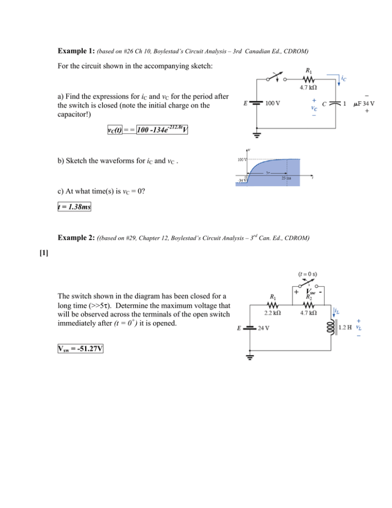
Example 1: (based on #26 Ch 10, Boylestad’s Circuit Analysis – 3rd Canadian Ed., CDROM) For the circuit shown in the accompanying sketch: a) Find the expressions for iC and vC for the period after the switch is closed (note the initial charge on the capacitor!) vC(t) = = 100 -134e-212.8tV b) Sketch the waveforms for iC and vC . c) At what time(s) is vC = 0? t = 1.38ms Example 2: ((based on #29, Chapter 12, Boylestad’s Circuit Analysis – 3rd Can. Ed., CDROM) [1] The switch shown in the diagram has been closed for a long time (>>5τ). Determine the maximum voltage that will be observed across the terminals of the open switch immediately after (t = 0+) it is opened. Vsw = -51.27V + Vsw - Example 3: (based on 2010 midterm) For the following waveform, determine the parameters listed below. 200 V 170V 180 160 140 120 a) The phase offset, φ , in degrees: φ = -360 100 80 60 40 20 -0.01 -0.005 0 -20 -40 t (s) 0.005 0.01 0.015 0.02 t = 1.6667ms -60 b) The peak-to-peak voltage: VP-P:340V -80 -100 -100V -120 -140 -160 -180 -200 c) The period. T: T: ______________________ T = 16.67ms d) The sinusoidal voltage v = 200 sin(2π1000t + 60°)V is plotted in (a) below; determine the time t1. t1 = .333ms e) The sinusoidal current i = 4 sin(50,000t - 40°)A is plotted in (b) below; determine the time t1. t1 = 13.96µs 0.025 Example 4: (based on #5, Chapter 15, Boylestad’s Circuit Analysis – 2nd Canadian Ed. CDROM) Calculate the total impedance of the circuits below. Express your answer in rectangular and polar forms, and draw the impedance diagrams showing each element and the total. a) Z = (3 –j3)Ω = 4.24∠-450Ω b) Z = (.5 +j3)kΩ = 3.04∠80.530 kΩ c) Z = (47 +j1617.7)Ω = 1618.4∠88.30Ω j j XL XL R XL j Z XL Z XL R R XC Z XC XC (a) (b) Example 5: ( Based on Boylestad’s 3rd Can. Ed. Ch. 15, Q10) For the circuit shown at right: a) Find the total impedance, ZT in polar form. ZT= 4.4472∠-63.435Ω b) Find the value of C (in µF) and L (in H). C = 265.25µF XL = 15.915mH (c) c) Find the current, I, and the voltages across each element in phasor notation and give the sinusoidal expression. j I = 11.18∠63.435A VR = 22.36∠63.435V = 31.608sin(377t+63.435o)V VL = 67.08∠153.435V = 94.865sin(377t +153.435o)V VC = 111.8∠-26.565V = 158.109sin(377t -26.565o)V IS VL VR E VC Example 6: (Based on Boylestad’s 3rd Can. Ed. Ch. 19, Q5) Consider the complex power loads connected to a 240V source as shown in the figure. Determine: a) The total real, reactive and apparent power. Draw the power triangle. b) Determine the source current, IS, and total impedance, ZT, seen by the source. c) Find the power factor, FP, for the combined loads as shown. d) Determine the type, value and VA rating of the reactive element needed to correct the power factor to 1. a) Load 1 2 3 4 total P(W) 300 1000 200 100 1600 Q(VAR) +400 +100 -500 -1200 -1200 S(VA) j Power Δ P=1600W θ =-36.87 S=2000VA 2000 b) I = 8.333∠96.87A ZT = 28.800∠-36.87Ω c) FP = 0.8leading. d) inductor L = 0.127H Rating: 240Volts, 1200VA Q=-1200VAR Example 7: (based on 2010 final) For the electric circuit shown below, find: ES, VL, the total power delivered to the load, RL, and the magnitude of the total impedance seen by the source, |ZS|. T1 ZS⇒ T2 0.5A ⇒ 100Ω ES 10Ω + VL 2:1 RL = 10Ω 3:1 PL = 22.5W 15V = VL; T1P = 100V; ZS = 80∠00Ω Example8: (based on 2010 final) The voltage source in the following diagram is 120VAC. Each of the two transformers has a 100 turn centre-tapped primary and secondary (i.e. 50 turns between each of the terminals on each winding). By making various connections between the source, transformers and load, different output voltages can be obtained. 120VAC 24Ω a) List all the possible output voltages that can be obtained by interconnecting the transformers. 30, 60, 120, 240, 480VAC b) On the diagram above, draw one connection option, using both transformers, that would result in 10A being delivered to the 24Ω load.
