lecture 260 – buffered op amps
advertisement
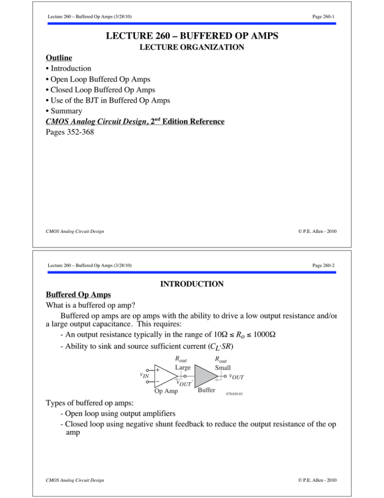
Lecture 260 – Buffered Op Amps (3/28/10) Page 260-1 LECTURE 260 – BUFFERED OP AMPS LECTURE ORGANIZATION Outline • Introduction • Open Loop Buffered Op Amps • Closed Loop Buffered Op Amps • Use of the BJT in Buffered Op Amps • Summary CMOS Analog Circuit Design, 2nd Edition Reference Pages 352-368 CMOS Analog Circuit Design © P.E. Allen - 2010 Lecture 260 – Buffered Op Amps (3/28/10) Page 260-2 INTRODUCTION Buffered Op Amps What is a buffered op amp? Buffered op amps are op amps with the ability to drive a low output resistance and/or a large output capacitance. This requires: - An output resistance typically in the range of 10 Ro 1000 - Ability to sink and source sufficient current (CL·SR) vIN + Rout Large Rout Small vOUT − vOUT’ Buffer Op Amp 070430-01 Types of buffered op amps: - Open loop using output amplifiers - Closed loop using negative shunt feedback to reduce the output resistance of the op amp CMOS Analog Circuit Design © P.E. Allen - 2010 Lecture 260 – Buffered Op Amps (3/28/10) Page 260-3 OPEN LOOP BUFFERED OP AMPS The Class A Source Follower as a Buffer VDD • Simple gm vIN M1 • Small signal gain g +g +G < 1 m mbs L vOUT • Low efficiency 1 VNBias1 • Rout = g +g 500 to 1000 M2 m mbs • Level shift from input to output 060118-10 • Maximum upper output voltage is limited • Broadbanded as the pole and zero due to the source follower are close so compensation is typically not a problem CMOS Analog Circuit Design © P.E. Allen - 2010 Lecture 260 – Buffered Op Amps (3/28/10) The Push-Pull Follower as a Buffer • Voltage loss from 2 cascaded followers gm3 gm1 Av gm3+gmbs3gm1+gmbs1+GL < 1 • Higher efficiency 0.5 • Rout gm+gmbs 250 to 500 • Current in M1 and M2 determined by: V GS4 + VSG3 = VGS1 + VSG2 2I6 Kn'(W 4/L4) + 2I5 Kp'(W 3/L3) Page 260-4 VDD VPBias1 M5 I5 M1 I1 + VSG3 V DD V + − GS1− M3 vIN vOUT VDD M4 VSG2 + VDD + VGS4 − − I6 I VNBias1 M2 2 M6 2I1 2I2 = + Kn'(W 1/L1) Kp'(W 2/L2) Use the W/L ratios to define I1 and I2 from I5 and I6 • Maximum positive and negative output voltages are limited CMOS Analog Circuit Design VDD 060706-02 © P.E. Allen - 2010 Lecture 260 – Buffered Op Amps (3/28/10) Page 260-5 Two-Stage Op Amp with Follower VDD M6 M3 - M4 M1 vin M8 Cc vout M2 CL + I7 M7 VNBiasM5 I5 M9 I9 060706-03 Power dissipation now becomes (I5 + I7 + I9)V DD Gain becomes, gm1 gm6 gm8 Av = gds2+gds4 gds6+gds7 gm8+gmbs8+gds8+gds9 CMOS Analog Circuit Design © P.E. Allen - 2010 Lecture 260 – Buffered Op Amps (3/28/10) Page 260-6 Source-Follower, Push-Pull Output Op Amp VDD M9 M6 IBias M12 M2 - M18 Cc M15 R1 M1 VSG18 + - M11 M7 M4 I17 M10 M5 R1 M8 + vin M17 R1 + VSS vout CL VSS VSG21 + - VGS19 I20 M16 M14 VSS + VDD V GS22 - M19 M13 M3 M22 VDD M21 M20 Buffer Fig. 7.1-1 1 Rout gm21+gm22 1000, Av(0)=65dB (IBias=50μA), and GB = 60MHz for CL = 1pF Note the bias currents through M18 and M19 vary with the signal. CMOS Analog Circuit Design © P.E. Allen - 2010 Lecture 260 – Buffered Op Amps (3/28/10) Page 260-7 Compensation of Op Amps with Output Amplifiers Compensation of a three-stage amplifier: Poles This op amp introduces a third pole, p’3 (what p1' and p2' about zeros?) + v2 With no compensation, + vin V out(s) -Avo = V in(s) s Unbuffered s s -1 -1 -1 op amp p’ p’ p’ 1 2 3 Illustration of compensation choices: jω vout x1 Output stage CL RL Fig. 7.1-4 jω p2 p3' Pole p3' Compensated poles Uncompensated poles p2' p2 σ p1' p1 p3=p3' p2' p1' p1 σ p3 Miller compensation applied around both the second and the third stage. Miller compensation applied around the second stage only. Fig. 7.1-5 CMOS Analog Circuit Design © P.E. Allen - 2010 Lecture 260 – Buffered Op Amps (3/28/10) Page 260-8 Crossover-Inverter, Buffer Stage Op Amp Principle: If the buffer has high output resistance and voltage gain (common source), this is okay if when loaded by a small RL the gain of this stage is approximately unity. VDD M7 M3 M4 M6 IBias C1 C2 vout RL vin + + - Input stage vin' M1 M2 M5 Cross over stage VSS Output Stage 060706-04 • This buffer trades gain for the ability to drive a low load resistance • The load resistance should be fixed in order to avoid changes in the buffer gain • The push-pull common source output will give good output voltage swing capability CMOS Analog Circuit Design © P.E. Allen - 2010 Lecture 260 – Buffered Op Amps (3/28/10) Page 260-9 Crossover-Inverter, Buffer Stage Op Amp - Continued How does the output buffer work? The two inverters, M1-M3 and M2-M4 are designed to work over different regions of the buffer input voltage, vin’. Consider the idealized voltage transfer characteristic of the crossover inverters: VDD IBias M7 M3 C1 vin' C2 M1 M5 M6 Active M2-M4 Inverter M1-M3 M6 SaturInverter M5 Saturated ated vout M2 vout VDD M6 M4 RL M5 Active 0 VSS VA VB VDD vin' 060706-05 VSS Crossover voltage VC = VB-V A 0 V C is designed to be small and positive for worst case variations in processing. CMOS Analog Circuit Design © P.E. Allen - 2010 Lecture 260 – Buffered Op Amps (3/28/10) Page 260-10 Large Output Current Buffer In the case where the load consists of a large capacitor, the ability to sink and source a large current is much more important than reducing the output resistance. Consequently, the common-source, push-pull is ideal if the quiescent current can be controlled. VDD A possible implementation: M5 VDD vin vout I=2Ib M7 M1 vout vin M3 M4 M8 If W4/L4 = W 9/L9 and W 3/L3 = W 8/L8, then the VSS quiescent currents in M1 and M2 can be determined by the following relationship: W /L W /L 1 1 2 2 I1 = I2 = Ib W 7/L7 = Ib W 10/L10 Ib M9 M2 M6 Ib I=2Ib VSS M10 070430-07 When vin is increased, M6 turns off M2 and turns on M1 to source current. Similarly, when vin is decreased, M5 turns off M1 and turns on M2 to sink current. CMOS Analog Circuit Design © P.E. Allen - 2010 Lecture 260 – Buffered Op Amps (3/28/10) Page 260-11 CLOSED LOOP BUFFERED OP AMPS Principle Use negative shunt feedback to reduce the output resistance of the buffer. vIN + − Ro ROUT vOUT Av RL 070430-02 • Output resistance Ro ROUT = 1+Av • Watch out for the case when RL causes Av to decrease. • The bandwidth will be limited by the feedback (i.e. at high frequencies, the gain of Av decreases causing the output resistance to increase. CMOS Analog Circuit Design © P.E. Allen - 2010 Lecture 260 – Buffered Op Amps (3/28/10) Page 260-12 Two Stage Op Amp with a Gain Boosted, Source Follower Buffer VDD 1:K M10 M6 M9 M3 - vin M4 M1 Cc M8 M2 + VNBiasM5 I5 M7 I7 Rout vout M11 I11 070430-03 1 Rout gm8K Power dissipation now becomes (I5 + I7 + I11)V DD Gain becomes, gm1 gm6 gm8K Av = gds2+gds4 gds6+gds7 gm8K+gmbs8K+GL CMOS Analog Circuit Design © P.E. Allen - 2010 Lecture 260 – Buffered Op Amps (3/28/10) Page 260-13 Gain Boosted, Source-Follower, Push-Pull Output Op Amp VDD + VT+2VON - M24 M9 M6 M8 IBias M11 VSG18 + - M12 M18 M7 M4 M23 M1 Cc M15 M2 R1 - + VGS19 - M22 VDD + VGS22 - Rout vout VSS VSG21 + I20 M16 M14 VSS 070430-04 M24 M19 M13 M3 1:K M23 I17 M10 M5 + vin M17 M20 M21 M25 M26 1:K Gain Enhanced Buffer 1000 1 Rout K(gm21+gm22) K 100 Av(0)=65dB (IBias=50μA) Note the bias currents through M18 and M19 vary with the signal. CMOS Analog Circuit Design © P.E. Allen - 2010 Lecture 260 – Buffered Op Amps (3/28/10) Page 260-14 Common Source, Push Pull Buffer with Shunt Feedback To get low output resistance using MOSFETs, negative feedback must be used. Ideal implementation: VDD Error Gain Amplifier Amplifier viin + - Error Amplifier M2 + iout vout + CL M1 VSS RL Fig. 7.1-5A Comments: • The output resistance will be equal to rds1||rds2 divided by the loop gain • If the error amplifiers are not perfectly matched, the bias current in M1 and M2 is not defined CMOS Analog Circuit Design © P.E. Allen - 2010 Lecture 260 – Buffered Op Amps (3/28/10) Page 260-15 Low Output Resistance Op Amp - Continued Offset correction circuitry: VDD + vin - + M6 M16 - -A1+ Cc VOS M9 vout Error Loop M8 Unbuffered op amp + VBias - - M10 M8A + A2 M17 M6A M12 M13 M11 VSS Fig. 7.1-6 The feedback circuitry of the two error amplifiers tries to insure that the voltages in the loop sum to zero. Without the M9-M12 feedback circuit, there is no way to adjust the output for any error in the loop. The circuit works as follows: When VOS is positive, M6 tries to turn off and so does M6A. IM9 reduces thus reducing IM12. A reduction in IM12 reduces IM8A thus decreasing VGS8A. VGS8A ideally decreases by an amount equal to VOS. A similar result holds for negative offsets and offsets in EA2. CMOS Analog Circuit Design © P.E. Allen - 2010 Lecture 260 – Buffered Op Amps (3/28/10) Page 260-16 Low Output Resistance Op Amp - Continued Error amplifiers: VDD M5A M6 M3 vin M4 Cc1 MR1 M1 M2 + VBias - M2A vout vin M1A MR2 Cc2 + M5 VBias A1 amplifier M6A VSS M4A M3A A2 amplifier 070430-05 Basically a two-stage op amp with the output push-pull transistors as the second-stage of the op amp. CMOS Analog Circuit Design © P.E. Allen - 2010 Lecture 260 – Buffered Op Amps (3/28/10) Page 260-17 Low Output Resistance Op Amp - Complete Schematic VDD + vin - M16 + - + VBiasP - M4H M3H M3 M5A MP3A MP4 MP5 M4 MP4A Cc M6 MP3 MR1 M9 M8A Cc2 Cc1 MR2 M10 M1 M2 M2A M1A MN3A M6A M8 M17 MN5A MN4 MN3 M5 M12 M13 + VBiasN - M3A M4A M11 M3HA MN4A M4HA VSS CC RC Short circuit protection(max. output ±60mA): MP3-MN3-MN4-MP4-MP5 MN3A-MP3A-MP4A-MN4A-MN5A rds6||rds6A 50k Rout LoopGain 5000 = 10 gm1 vout Fig. 7.1-8 gm6 R1 C1 RL CMOS Analog Circuit Design CL © P.E. Allen - 2010 Lecture 260 – Buffered Op Amps (3/28/10) Page 260-18 Simpler Implementation of Negative Feedback to Achieve Low Output Resistance VDD + vin - M8 M3 1/1 10/1 200μA M4 M1 10/1 M2 M6 1/1 10/1 vout Output Resistance: Ro R = out 1+LG CL where 10/1 1/1 M5 M10 1/1 10/1 M9 M7 VSS Rout = and 10/1 Fig. 7.1-9 1 Ro = gds6+gds7 gm2 |LG| = 2gm4 (gm6+gm7)Ro Therefore, the output resistance is: 1 gm2 (gds6+gds7) 1+ 2gm4(gm6+gm7)Ro CMOS Analog Circuit Design © P.E. Allen - 2010 Lecture 260 – Buffered Op Amps (3/28/10) Page 260-19 Example 260-1 - Low Output Resistance Using Shunt Negative Feedback Buffer Find the output resistance of above op amp using the model parameters of KN’ = 120μA/V2, KP’ = 25μA/V2, N = 0.06V-1 and P = 0.08V-1. Solution The current flowing in the output transistors, M6 and M7, is 1mA which gives Ro of 1 1000 Ro = ( + )1mA = 0.14 = 7.143k N P To calculate the loop gain, we find that gm2 = 2KN’·10·100μA = 490μS gm4 = 2KP’·1·100μA = 70.7μS and gm6 = 2KP’·10·1000μA = 707μS Therefore, the loop gain is 490 |LG| = 2·70.7 (0.707+0.071)7.143 = 19.26 Solving for the output resistance, Rout, gives 7.143k Rout = 1+19.26 = 353 (Assumes that RL is large) CMOS Analog Circuit Design © P.E. Allen - 2010 Lecture 260 – Buffered Op Amps (3/28/10) Page 260-20 USE OF THE BJT IN BUFFERED OP AMPS Substrate BJTs Illustration of an NPN substrate BJT available in a p-well CMOS technology: ;;; ;; ; ;;; ;;; Emitter n+ (Emitter) Base p+ p- well (Base) Collector (VDD) n+ Collector (VDD) Base n- substrate (Collector) Fig. 7.1-10 Emitter Comments: • gm of the BJT is larger than the FET so that the output resistance w/o feedback is lower • Collector current will be flowing in the substrate • Current is required to drive the BJT • Only an NPN or a PNP bipolar transistor is available CMOS Analog Circuit Design © P.E. Allen - 2010 Lecture 260 – Buffered Op Amps (3/28/10) Page 260-21 A Lateral Bipolar Transistor n-well CMOS technology: • It is desirable to have the lateral collector current much larger than the vertical collector current. • Triple well technology allows the current of the vertical collector to avoid flowing in the substrate. • Lateral BJT generally has good matching. B VC E LC n+ LC p+ p+ p+ STI STI n-well Substrate 060221-01 Vertical Collector STI Lateral Collector Emitter Base CMOS Analog Circuit Design © P.E. Allen - 2010 Lecture 260 – Buffered Op Amps (3/28/10) A Field-Aided Lateral BJT Use minimum channel length to enhance beta: ßF 50 to 100 depending on the process Page 260-22 VC STI B LC E LC n+ p+ p+ pp++ Keeps carriers from flowing at the surface and reduces 1/f noise n-well STI Substrate 060221-02 Vertical Collector STI Lateral Collector Emitter Base CMOS Analog Circuit Design © P.E. Allen - 2010 Lecture 260 – Buffered Op Amps (3/28/10) Page 260-23 Two-Stage Op Amp with a Class-A BJT Output Buffer Stage VDD Purpose of the M8-M9 source follower: M5 M7 M12 M8 1.) Reduce the output resistance + Q10 vin (includes whatever is seen from M1 M2 the base to ground divided by vout IBias M9 1+F) Cc M4 CL RL M3 2.) Reduces the output load at the M6 M13 M11 drains of M6 and M7 Output Buffer VSS Fig. 7.1-11 Small-signal output resistance : r10+(1/gm9) 1 1 Rout = g + g (1+ß ) 1+ßF m10 m9 F = 51.6+6.7 = 58.3 where I10=500μA, I8=100μA, W9/L9=100 and ßF is 100 2KP’ Ic10 vOUT(max) = VDD - VSD8(sat) - vBE10 = VDD I8(W 8/L8) - Vt lnIs10 Voltage gain: gm9 vout gm1 gm6 gm10RL vin gds2+gds4gds6+gds7gm9+gmbs9+gds8+g101+gm10RL Compensation will be more complex because of the additional stages. CMOS Analog Circuit Design Lecture 260 – Buffered Op Amps (3/28/10) © P.E. Allen - 2010 Page 260-24 Example 260-2 - Designing the Class-A, Buffered Op Amp Use an n-well, 0.25μm CMOS technology to design an op amp using a class-A, BJT output stage to give the following specifications. Assume the channel length is to be 0.5μm. The FETs have the model parameters of KN’ = 120μA/V2, KP’ = 25μA/V2, VTN = |VTP| = 0.5V, N = 0.06V-1 and P = 0.08V-1 along with the BJT parameters of Is = 10-14A and ßF = 50. V DD = 2.5V V SS = 0V GB = 5MHz Avd(0) 2500V/V Slew rate 10V/μs Rout 50 CL = 100pF ICMR = +1V to 2V RL = 500 Solution VDD A quick comparison shows that the VPB1 VPB1 M14 specifications of this problem are similar I4 I5 to the folded cascode op amp that was I15 M4 M5 designed in Ex. 240-3. Borrowing that Rout vO VPB2 design for this example results in the I1 I2 I12 I6 I7 following op amp. C M6 M7 Therefore, the goal of this example + M12 M1 M2 VNB2 will be the design of M12 through Q15 to vIN M9 M8 Q15 satisfy the slew rate and output resistance − M11 V M3 NB1 I3 requirements. VNB1 M10 M13 070430 CMOS Analog Circuit Design © P.E. Allen - 2010 Lecture 260 – Buffered Op Amps (3/28/10) Page 260-25 Example 260-2 – Continued BJT follower (Q15): SR = 10V/μs and 100pF capacitor give I15 = 1mA. Assuming the gate of M14 is connected to the gate of M5, the W /L ratio of M14 becomes W 14/L14 = (1000μA/125μA)160 = 1280 W 14 = 640μm I15 = 1mA 1/gm15 = 0.0258V/1mA = 25.8 MOS follower: To source 1mA, the BJT requires 20μA (ß =50) from the MOS follower (M12-M13). Therefore, select a bias current of 100μA for M13. If the gates of M3 and M13 are connected together, then W 13/L13 = (100μA/100μA)15 = 15 W 13 = 7.5μm To get Rout = 50, if 1/gm15 is 25.8, then design gm12 as 1 1 1 1 = 24.2 gm12 = (24.2)(1+ßF) = 24.2·51 = 810μS gm15 = gm12(1+ßF) gm12 and I12 W/L = 27.3 30 W 12 = 15μm CMOS Analog Circuit Design Lecture 260 – Buffered Op Amps (3/28/10) © P.E. Allen - 2010 Page 260-26 Example 260-2 - Continued To calculate the voltage gain of the MOS follower we need to find gmbs9 (N = 0.4 V). gm12N 810·0.4 = = 158μS gmbs12 = 2 2F+VBS12 2 0.5+0.55 where we have assumed that the value of VSB12 is approximately 1.25V – 0.7V = 0.55V. 810μS AMOS = 810μS+158μS+6μS+8μS = 0.825 The voltage gain of the BJT follower is 500 ABJT = 25.8+500 = 0.951 V/V Thus, the gain of the op amp is Avd(0) = (3,678)(0.825)(0.951) = 2,885 V/V The power dissipation of this amplifier is, Pdiss. = 2.5V(125μA+125μA+100μA+1000μA) = 3.375mW The signal swing across the 500 load resistor will be restricted to ±0.5V due to the 1000μA output current limit. CMOS Analog Circuit Design © P.E. Allen - 2010 Lecture 260 – Buffered Op Amps (3/28/10) • • • • Page 260-27 SUMMARY A buffered op amp requires an output resistance between 10 Ro 1000 Output resistance using MOSFETs only can be reduced by, - Source follower output (1/gm) - Negative shunt feedback (frequency is a problem in this approach) Use of substrate (or lateral) BJT’s can reduce the output resistance because gm is larger than the gm of a MOSFET Adding a buffer stage to lower the output resistance will most likely complicate the compensation of the op amp CMOS Analog Circuit Design © P.E. Allen - 2010
