0.5 – 4 GHz 3 V Low Current GaAs MMIC LNA Technical Data
advertisement
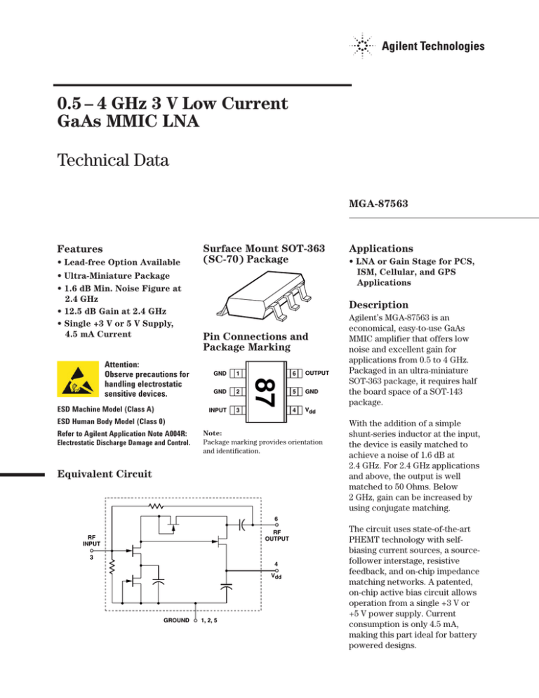
0.5 – 4 GHz 3 V Low Current GaAs MMIC LNA Technical Data MGA-87563 Features • Lead-free Option Available • Ultra-Miniature Package • 1.6 dB Min. Noise Figure at 2.4 GHz • 12.5 dB Gain at 2.4 GHz • Single +3 V or 5 V Supply, 4.5 mA Current ESD Machine Model (Class A) Pin Connections and Package Marking GND 1 GND 2 INPUT 3 MGA-87563 Pkg 6 OUTPUT 5 GND 4 Vdd ESD Human Body Model (Class 0) Refer to Agilent Application Note A004R: Electrostatic Discharge Damage and Control. Applications • LNA or Gain Stage for PCS, ISM, Cellular, and GPS Applications Description 87 Attention: Observe precautions for handling electrostatic sensitive devices. Surface Mount SOT-363 (SC-70) Package Note: Package marking provides orientation and identification. Equivalent Circuit Agilent’s MGA-87563 is an economical, easy-to-use GaAs MMIC amplifier that offers low noise and excellent gain for applications from 0.5 to 4 GHz. Packaged in an ultra-miniature SOT-363 package, it requires half the board space of a SOT-143 package. With the addition of a simple shunt-series inductor at the input, the device is easily matched to achieve a noise of 1.6 dB at 2.4 GHz. For 2.4 GHz applications and above, the output is well matched to 50 Ohms. Below 2 GHz, gain can be increased by using conjugate matching. 6 RF OUTPUT RF INPUT 3 4 Vdd GROUND 1, 2, 5 The circuit uses state-of-the-art PHEMT technology with selfbiasing current sources, a sourcefollower interstage, resistive feedback, and on-chip impedance matching networks. A patented, on-chip active bias circuit allows operation from a single +3 V or +5 V power supply. Current consumption is only 4.5 mA, making this part ideal for battery powered designs. 2 Absolute Maximum Ratings Symbol Parameter Units Absolute Maximum[1] Vdd Device Voltage, RF Output to Ground V 6 Vin Vout RF input or RF Output Voltage to Ground V +0.5 –1.0 Pin CW RF Input Power dBm +13 Tch Channel Temperature °C 150 TSTG Storage Temperature °C -65 to 150 Thermal Resistance[2]: θch-c = 160°C/W Notes: 1. Operation of this device above any one of these limits may cause permanent damage. 2. TC = 25°C (TC is defined to be the temperature at the package pins where contact is made to the circuit board). MGA-87563 Electrical Specifications[3], TC = 25°C, ZO = 50 Ω, Vdd = 3 V Symbol Parameters and Test Conditions Gtest[3] NFtest Units f = 2.0 GHz [3] Min. Typ. 11 14 f = 2.0 GHz 1.8 NFo Optimum Noise Figure (Tuned for lowest noise figure) f = 0.9 GHz f = 1.5 GHz f = 2.0 GHz f = 2.4 GHz f = 4.0 GHz dB 1.9 1.6 1.6 1.6 2.0 Ga Associated Gain at NFO (Tuned for lowest noise figure) f = 0.9 GHz f = 1.5 GHz f = 2.0 GHz f = 2.4 GHz f = 4.0 GHz dB 14.6 14.5 14.0 12.5 10.3 P1dB Output Power at 1 dB Gain Compression f = 0.9 GHz f = 1.5 GHz f = 2.0 GHz f = 2.4 GHz f = 4.0 GHz dBm -2.0 -1.8 -2.0 -2.0 -2.6 IP3 Third Order Intercept Point f = 2.4 GHz dBm +8 Output VSWR f = 2.4 GHz VSWR Idd Device Current 1.8 mA Note: 3. Guaranteed specifications are 100% tested in the circuit in Figure 10 in the Applications Information section. 4.5 Max. 2.3 3 MGA-87563 Typical Performance, TC = 25°C, Vdd = 3 V 20 ASSOCIATED GAIN (dB) 3 +85 2 +25 1 -40 0 0.5 1.0 1.5 2.0 2.5 3.0 3.5 -40 +25 +85 10 5 0 0.5 4.0 -1 15 1.0 FREQUENCY (GHz) 2.5 3.0 3.5 2 1.5 2.0 2.5 3.0 -3 -5 0.5 4.0 3.5 3.3 V 3.0 V 2.7 V 10 2.5 OUTPUT 2.0 1.5 1.0 1.5 2.0 2.5 3.0 3.5 -5 0.5 4.0 2.0 2.5 3.0 1.0 3.5 FREQUENCY (GHz) Figure 7. Input and Output VSWR (into 50 Ω) vs. Frequency. 4.0 15 4.0 3.5 Ga 50 10 3.0 NF 50 2.5 5 2.0 1.0 0.5 1.0 NF OPT 1.5 2.0 2.5 3.0 1.5 2.5 2.0 3.0 3.5 4.0 FREQUENCY (GHz) Figure 6. Output Power for 1 dB Gain Compression (into 50 Ω) vs. Frequency and Voltage. 6 20 1.5 1.5 3.3 V 3.0 V 2.7 V -3 3.5 FREQUENCY (GHz) Figure 8. 50 Ω Noise Figure and Associated Gain vs. Frequency. 0 4.0 5 CURRENT (mA) NOISE FIGURE (dB) INPUT 4.0 -2 4.5 3.0 3.5 -4 5.0 3.5 3.0 5 Figure 5. Associated Gain (Optimum Tuning) vs. Frequency and Voltage. 4.0 2.5 -1 FREQUENCY (GHz) Figure 4. Minimum Noise Figure (Optimum Tuning) vs. Frequency and Voltage. 2.0 Figure 3. Output Power for 1 dB Gain Compression (into 50 Ω) vs. Frequency and Temperature. 15 0 0.5 4.0 1.5 0 FREQUENCY (GHz) 1.0 1.0 FREQUENCY (GHz) P 1dB (dBm) 3.3 V 3.0 V 2.7 V ASSOCIATED GAIN (dB) NOISE FIGURE (dB) 3 1 VSWR (n:1) 2.0 20 4 1.0 0.5 1.5 Figure 2. Associated Gain (Optimum Tuning) vs. Frequency and Temperature. 5 1.0 -40 +25 +85 FREQUENCY (GHz) Figure 1. Minimum Noise Figure (Optimum Tuning) vs. Frequency and Temperature. 0 0.5 -2 -4 ASSOCIATED GAIN (dB) NOISE FIGURE (dB) 4 0 P 1 dB (dBm) 5 4 +85 +50 +25 0 -40 3 2 1 0 0 1 2 3 4 VOLTAGE (V) Figure 9. Device Current vs. Voltage. 5 4 MGA-87563 Typical Scattering Parameters[4], TC = 25°C, ZO = 50 Ω, Vdd = 3 V Freq. GHz Mag 0.1 0.92 0.2 S11 Ang dB S21 Mag Ang dB S12 Mag Ang Mag Ang K Factor -5 -5.6 0.53 -90 -22.7 0.073 -7 0.86 -11 0.41 0.91 -8 -0.7 0.92 -100 -22.7 0.073 -9 0.85 -18 0.29 0.5 0.88 -20 6.7 2.15 -131 -23.4 0.068 -18 0.78 -43 0.33 1.0 0.79 -35 10.1 3.22 -170 -25.2 0.055 -26 0.61 -75 0.72 1.5 0.73 -49 11.2 3.63 163 -26.2 0.049 -33 0.50 -100 1.02 2.0 0.67 -60 11.4 3.72 140 -26.6 0.047 -39 0.42 -122 1.32 2.5 0.59 -69 11.0 3.54 119 -29.1 0.035 -40 0.31 -141 2.38 3.0 0.50 -78 10.7 3.41 101 -32.5 0.024 -52 0.25 -167 4.29 3.5 0.43 -83 10.1 3.20 85 -35.1 0.018 -12 0.20 172 6.74 4.0 0.37 -96 10.0 3.16 71 -37.7 0.013 -10 0.24 143 9.83 4.5 0.31 -91 8.7 2.72 52 -26.1 0.050 20 0.11 123 3.33 5.0 0.30 -105 8.1 2.55 42 -25.9 0.050 -3 0.17 127 3.48 MGA-87563 Typical Noise Parameters[4], TC = 25°C, ZO = 50 Ω, Vdd = 3 V Γopt Frequency (GHz) NFo (dB) Mag. Ang. RN/50 Ω 0.5 2.6 0.71 1 1.57 1.0 1.7 0.68 17 0.96 1.5 1.6 0.68 28 0.75 2.0 1.6 0.66 36 0.67 2.5 1.6 0.63 42 0.56 3.0 1.6 0.59 49 0.53 3.5 1.8 0.56 55 0.55 4.0 2.0 0.53 62 0.58 Notes: 4. Reference plane per Figure 11 in Applications Information section. S22 5 MGA-87563 Applications Information Introduction The MGA-87563 low noise RF amplifier is designed to simplify wireless RF applications in the 0.5 to 4 GHz frequency range. The MGA-87563 is a two-stage, GaAs Microwave Monolithic Integrated Circuit (MMIC) amplifier that uses feedback to provide wideband gain. The output is matched to 50 Ω and the input is partially matched for optimum noise figure. A patented, active bias circuit makes use of current sources to “re-use” the drain current in both stages of gain, thus minimizing the required supply current and decreasing sensitivity to variations in power supply voltage. Test Circuit The circuit shown in Figure 10 is used for 100% RF testing of Noise Figure and Gain. The input of this circuit is fixed tuned for a conjugate power match (maximum power transfer, or, minimum Input VSWR) at 2 GHz. Tests in this circuit are used to guarantee the NFtest and Gtest parameters shown in the Electrical Specifications table. The 4.7 nH inductor, L1 (Coilcraft, Cary, IL part number series 1008CT-040) placed in series with C1 Vdd 4.7 nH Biasing The MGA-87563 is a voltagebiased device and operates from a single +3 volt power supply. With a typical current drain of only 4.5 mA, the MGA-87563 is very well suited for use in battery powered applications. All bias regulation circuitry is integrated into the MMIC, eliminating the need for external DC components. RF performance is very consistent for 3-volt battery supplies that may range from 2.7 to 3.3 volts, depending on battery “freshness” or state of charge for rechargeable batteries. Operation up to +5 volts is discussed at the end of the Applications section. The test circuit in Figure 10 illustrates a suitable method for bringing bias into the MGA-87563. The bias connection must be designed so that it adequately bypasses the Vdd terminal while not inadvertently creating any resonances at frequencies where the MGA-87563 has gain. RF OUTPUT L1 50 Ω Phase Reference Planes The positions of the reference planes used to measure S-Parameters and to specify Γopt for the Noise Parameters are shown in Figure 11. As seen in the illustration, the reference planes are located at the extremities of the package leads. REFERENCE PLANES 10 Ω RF INPUT the input of the amplifier is all that is necessary to match the input to 50 Ω at 2 GHz. 50 Ω TEST CIRCUIT Figure 10. Test Circuit for 2 GHz. Figure 11. Reference Planes. The 10 Ω resistor, R1, serves to “de-Q” any potential resonances in the bias line that could lead to low gain, unwanted gain variations or device instability. The power supply end of R1 is bypassed to ground with capacitor C1. The suggested value for C1 is 100 pF. Significantly higher values for C1 are not recommended. Many higher value chip capacitors (e.g., 1000 pF) are not of sufficiently high quality at these frequencies to function well as a RF bypass without adding harmful parasitics or selfresonances. While the input and output terminals are internally resistively grounded, these pins should not be considered to be current sinks. Connection of the MGA-87563 amplifier to circuits that are at ground potential may be made without the additional cost and PCB space needed for DC blocking capacitors. If the amplifier is to be cascaded with active circuits having non-zero voltages present, the use of series blocking capacitors is recommended. Input Matching The input of the MGA-87563 is partially matched internally to 50 Ω. The use of a simple input conjugate matching circuit (such as shown in Figure 10 for 2 GHz), will lower the noise figure considerably. A significant advantage of the MGA-87563’s design is that the impedance match for NFo (minimum noise figure) is very close to a conjugate power match. This means that a very low noise figure can be realized simultaneously with a low input VSWR. The typical difference 6 between the noise figure obtainable with a conjugate power match at the input and NFo is only about 0.2 dB. Output Matching The output of the MGA-87563 is matched internally to 50 Ω above 1.8 GHz. The use of a conjugate matching circuit, such as a simple series inductor, can increase the gain considerably at lower frequencies. Matching the output will not affect the noise figure. Stability If the MGA-87563 is cascaded with highly reactive stages (such as filters) some precautions may be needed to ensure stability. The low frequency stability (under 1.5 GHz) of the MGA-87563 can be enhanced by adding a series R-L network in shunt with the output, as shown in Figure 12. The inductor can be either a chip component or a high impedance transmission line as shown in the figure. Component values are selected such that the output of the MGA-87563 will be resistively loaded at low frequencies while allowing high frequency signals to pass the stability load with minimal loss. 0.020 inches, using 0.031-inch thick FR-4 (εr = 4.8) circuit board as the substrate. For applications near 1.5 GHz, gain (and output power) may be traded off for increased stability. Some precautions regarding the Vdd connection of the MGA-87563 are also recommended to ensure stability within the operating frequency range of the device. It is important that the connection to the power supply be properly bypassed to realize full amplifier performance. Refer to the Biasing section above for more information. SOT-363 PCB Layout A PCB pad layout for the miniature SOT-363 (SC-70) package is shown in Figure 13 (dimensions are in inches). This layout provides ample allowance for package placement by automated assembly equipment without adding parasitics that could impair the high frequency RF performance of the MGA-87563. The layout is shown with a nominal SOT-363 package footprint superimposed on the PCB pads. 0.026 Typical values for the resistor are in the 25 to 50 Ω range. A suggested starting place for the inductor is a 0.35 to 0.40-inch long microstripline with a width of DC BLOCKING CAPACITOR MGA 87563 25-50 Ω RF OUTPUT HIGH IMPEDANCE TRANSMISSION OR INDUCTOR Figure 12. Output Circuitry for Low Frequency Stability. 0.079 0.039 RF Layout The RF layout in Figure 14 is suggested as a starting point for designs using the MGA-87563 amplifier. Adequate grounding is needed to obtain maximum performance and to obviate potential instability. All three ground pins of the MMIC should be connected to RF ground by using plated through holes (vias) near the package terminals. It is recommended that the PCB traces for the ground pins NOT be connected together underneath the body of the package. PCB pads hidden under the package cannot be adequately inspected for SMT solder quality. FR-4 or G-10 PCB material is a good choice for most low cost wireless applications. Typical board thickness is 0.025 or 0.031 inches. The width of 50 Ω microstriplines in these PCB thicknesses is also convenient for mounting chip components such as the series inductor at the input for impedance matching or for DC blocking capacitors. For noise figure sensitive applications, the use of PTFE/glass dielectric materials may be warranted to minimize transmission line losses at the amplifier input. Higher Bias Voltages While the MGA-87563 is designed for use in +3 volt battery powered applications, the internal bias regulation circuitry allows it to be VDD 0.018 Dimensions in inches. Figure 13. Recommended PCB Pad Layout for Agilent’s SC70 6L/SOT-363 Products. RF OUTPUT 50 Ω 87 50 Ω RF INPUT Figure 14. RF Layout. 7 easily operated with any power supply voltage from +2.7 to 5 volts. Figure 15 shows an increase of approximately 1 dB in the associated gain with +5 volts applied. The P1dB output power (Figure 17) is also higher by about 1 dBm. The effect of higher Vdd on noise figure is negligible as indicated in Figure 16. Package Dimensions Outline 63 (SOT-363/SC-70) HE E e 17 D ASSOCIATED GAIN (dB) 16 15 14 Q1 A2 13 12 A c A1 11 9 0.5 1.0 1.5 2.0 2.5 3.0 3.5 4.0 DIMENSIONS (mm) FREQUENCY (GHz) SYMBOL E D HE A A2 A1 Q1 e b c L Figure 15. Associated Gain vs. Frequency at Vdd = 5 Volts. 3.5 3.0 OPTIMUM NF (dB) L b 10 2.5 2.0 MAX. 1.35 2.25 2.40 1.10 1.00 0.10 0.40 MIN. 1.15 1.80 1.80 0.80 0.80 0.00 0.10 NOTES: 1. All dimensions are in mm. 2. Dimensions are inclusive of plating. 3. Dimensions are exclusive of mold flash & metal burr. 4. All specifications comply to EIAJ SC70. 5. Die is facing up for mold and facing down for trim/form, ie: reverse trim/form. 6. Package surface to be mirror finish. 0.650 BCS 0.15 0.10 0.10 0.30 0.20 0.30 1.5 1.0 0.5 0.5 1.0 1.5 2.0 2.5 3.0 3.5 4.0 Part Number Ordering Information FREQUENCY (GHz) Figure 16. Optimum Noise Figure vs. Frequency at Vdd = 5 Volts. 0.00 P 1 dB (dBm) -0.50 -1.00 No. of Devices 3000 Container 7" Reel MGA-87563-TR2 MGA-87563-BLK 10000 100 13" Reel antistatic bag MGA-87563-TR1G MGA-87563-TR2G 3000 10000 7" Reel 13" Reel MGA-87563-BLKG 100 antistatic bag Note: For lead-free option, the part number will have the character “G” at the end. -1.50 -2.00 0.6 Part Number MGA-87563-TR1 1.2 1.8 2.4 3.0 3.6 4.2 FREQUENCY (GHz) Figure 17. Output Power at 1 dB Gain Compression vs. Frequency at Vdd = 5 Volts. Device Orientation REEL TOP VIEW END VIEW 4 mm CARRIER TAPE 8 mm 87 87 87 87 USER FEED DIRECTION COVER TAPE Tape Dimensions and Product Orientation For Outline 63 P P2 D P0 E F W C D1 t1 (CARRIER TAPE THICKNESS) Tt (COVER TAPE THICKNESS) K0 10° MAX. A0 DESCRIPTION 10° MAX. B0 SYMBOL SIZE (mm) SIZE (INCHES) CAVITY LENGTH WIDTH DEPTH PITCH BOTTOM HOLE DIAMETER A0 B0 K0 P D1 2.40 ± 0.10 2.40 ± 0.10 1.20 ± 0.10 4.00 ± 0.10 1.00 + 0.25 0.094 ± 0.004 0.094 ± 0.004 0.047 ± 0.004 0.157 ± 0.004 0.039 + 0.010 PERFORATION DIAMETER PITCH POSITION D P0 E 1.55 ± 0.10 4.00 ± 0.10 1.75 ± 0.10 0.061 + 0.002 0.157 ± 0.004 0.069 ± 0.004 CARRIER TAPE WIDTH THICKNESS W t1 8.00 + 0.30 - 0.10 0.254 ± 0.02 0.315 + 0.012 0.0100 ± 0.0008 For product information and a complete list of Agilent contacts and distributors, please go to our web site. COVER TAPE WIDTH TAPE THICKNESS C Tt 5.40 ± 0.10 0.062 ± 0.001 0.205 + 0.004 0.0025 ± 0.0004 www.agilent.com/semiconductors DISTANCE CAVITY TO PERFORATION (WIDTH DIRECTION) F 3.50 ± 0.05 0.138 ± 0.002 CAVITY TO PERFORATION (LENGTH DIRECTION) P2 2.00 ± 0.05 0.079 ± 0.002 E-mail: SemiconductorSupport@agilent.com Data subject to change. Copyright © 2004 Agilent Technologies, Inc. Obsoletes 5965-9688E November 16, 2004 5989-1803EN

