University of California at Berkeley College of Engineering
advertisement

University of California at Berkeley
College of Engineering
Department of Electrical Engineering and Computer Sciences
EECS150
Spring 2000
J. Wawrzynek
E. Caspi
Homework #4 – Solution
1. We implement a rightward bit rotator using tri-states. Given a 4-bit input
{x3 x2 x1 x0} and a one-hot-encoded rotation amount {s3 s2 s1 s0}, the bit rotator
produces output {y3 y2 y1 y0} as follows:
Rotation
{s3 s2 s1 s0}
0001
0010
0100
1000
{y3
{x3
{x0
{x1
{x2
Output
y2 y1
x2 x1
x3 x2
x0 x3
x1 x0
y0}
x0}
x1}
x2}
x3}
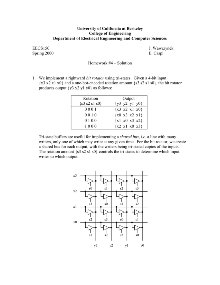
Tri-state buffers are useful for implementing a shared bus, i.e. a line with many
writers, only one of which may write at any given time. For the bit rotator, we create
a shared bus for each output, with the writers being tri-stated copies of the inputs.
The rotation amount {s3 s2 s1 s0} controls the tri-states to determine which input
writes to which output.
x3
x2
x1
x0
s0
s1
s2
s3
s3
s0
s1
s2
s2
s3
s0
s1
s1
s2
s3
s0
y3
y2
y1
y0
2. A basic 4x4 memory memory structure needs 4 rows (1 row per address) and 4
columns (1 per bit of output). The address input is decoded into a one-hot collection
of “row-select” bits used to activate whichever row corresponds to the address. The
cells of the active row then write onto vertical bit lines to produce the output data. To
make this structure dual ported, we duplicate the address input, row-select lines, and
bit lines. Each cell must now have two separate tri-states for output.
Row-select
Bit
line
Address #2
2-to-4 Decoder
Address #1
2-to-4 Decoder
Single-ported ROM cell
Dual-ported ROM cell
Problem #2:
4x4 ROM
D13 D12 D11 D10
D23 D22 D21 D20
Data out #1
Data out #2
3.
The process of creating a large memory from smaller ones is an extension of the
process of creating a basic memory from bit cells. We create one row per
multiplicative increase in the number of addresses, and one column per multiplicative
increase in the number of data bits. To create a 4Mbit 4 RAM from 1Mbit 1
components, we need 4 rows (to quadrouple the address space) and 4 columns (to
quadrouple the data width). We give the 4Mbit 4 RAM an interface analogous to
that of the 1Mbit 1 component: 22 address bits, 4 data bits, WE, and OE. For each
row of 1Mbit 1 components, we generate WErow and OErow by AND-ing the global
signals WE and OE with a row-specific “row-select” signal generated by decoding
the top two address bits.
1M 1
1M 1
1M 1
1M 1
OE WE A D
OE WE A D
OE WE A D
OE WE A D
1M 1
1M 1
1M 1
1M 1
OE WE A D
OE WE A D
OE WE A D
OE WE A D
1M 1
1M 1
1M 1
1M 1
OE WE A D
OE WE A D
OE WE A D
OE WE A D
1M 1
1M 1
1M 1
1M 1
OE WE A D
OE WE A D
OE WE A D
OE WE A D
20 addr[19:0]
2
addr[21:20]
OE0
WE0
2-to-4 Decoder
OE1
WE1
OE2
WE2
OE3
WE3
OE
WE
data[3:0]
It is possible to simplify the interface for the 4Mbit 4 RAM by removing the global
OE signal. In such a configuration, the global WE alone determines the read/write
mode: high for a write, low for a read. Each row gets: WErow = WE AND row-select,
and OErow = (WE)’ AND row-select. Note that a memory in this configuration can no
longer be easily composed into yet larger memories.
4. We have seen in lecture that the delay of a transmission line increases with the square
of its length: = kL2 (for some constant k). Introducing a buffer in the middle of a
transmission line splits it into two halves, each with delay: 1/2 = k (L/2)2. The total
delay through both halves plus the buffer is:
buffered = 21/2 + buffer
= 2k (L/2)2 + buffer
= (1/2)k L2 + buffer
= (1/2) + buffer
When a wire is long enough to be treated as a transmission line, its parasitic effects
are more significant than a single buffer delay (i.e.: » buffer). Thus we can ignore
the buffer delay and approximate: buffered = (1/2).
The so-called time constant of a circuit is the time it takes for a signal transition to
complete (1-1/e) 63% of its level change. This time constant is often used as a
measure of characteristic delay. For a transmission line dominated by resistive and
capacitive effects – assuming a length L, resistance R/L Ohms per unit length, and
capacitance C/L Farads per unit length – the time constant is: = (R/L)(C/L)L2/2, or
more simply: = k L2, with constant k = (R/L)(C/L)/2. Thus the time constant of a
transmission line increases with the square of its length.


