TABLE OF CONTENTS
advertisement
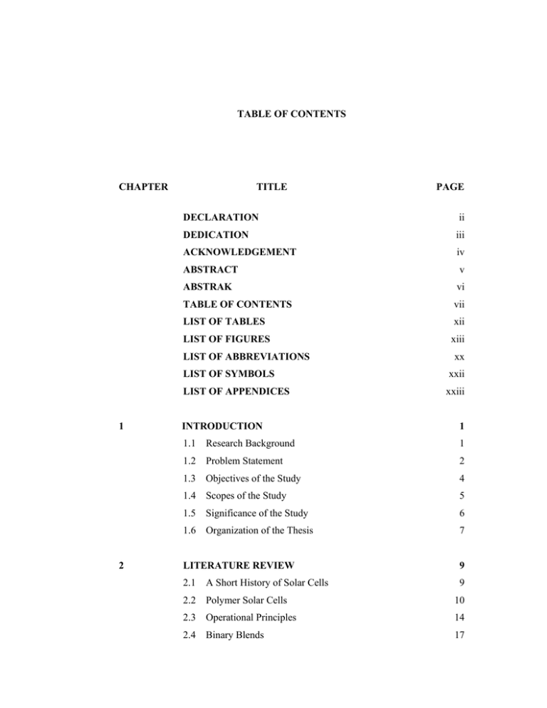
TABLE OF CONTENTS CHAPTER TITLE DECLARATION ii DEDICATION iii ACKNOWLEDGEMENT iv ABSTRACT v ABSTRAK vi TABLE OF CONTENTS vii LIST OF TABLES xii LIST OF FIGURES xiii LIST OF ABBREVIATIONS 1 2 PAGE xx LIST OF SYMBOLS xxii LIST OF APPENDICES xxiii INTRODUCTION 1 1.1 Research Background 1 1.2 Problem Statement 2 1.3 Objectives of the Study 4 1.4 Scopes of the Study 5 1.5 Significance of the Study 6 1.6 Organization of the Thesis 7 LITERATURE REVIEW 9 2.1 A Short History of Solar Cells 9 2.2 Polymer Solar Cells 10 2.3 Operational Principles 14 2.4 Binary Blends 17 viii 2.5 Ternary Blends 2.5.1 Polymer: Polymer: Fullerene Ternary Blend 21 23 2.5.2 Charge Transfer and Transport Mechanism in Ternary Solar Cells 2.6 Controlling the Active Layer Morphology 28 2.6.1 Solvent Effects 29 2.6.2 Annealing Treatment 31 2.6.3 Donor to Acceptor Ratio 36 2.7 Processing of the Devices 2.7.1 Coating Methods 2.7.1.1 Spray Coating 3 27 39 42 42 RESEARCH METHODOLOGY 51 3.1 Research Design and Procedure 51 3.2 Material Selection 54 3.2.1 Active Layer 54 3.2.2 Solvents 55 3.2.3 Electron Transport Layer and Hole Transport Layer 56 3.3 Fabrication of Thin Films 57 3.4 Fabrication of Polymer Solar Cells 58 3.5 Spray Coating and Spin Coating Methods 59 3.6 61 Post-deposition Treatment 3.7 Characterization and Performance Testing 63 3.7.1 UV-Vis Spectrophotometer 65 3.7.2 Photoluminescence (PL) Spectroscopy 65 3.7.3 Atomic Force Microscopy 66 3.7.4 Optical Microscopy 67 3.7.5 X-ray Diffractometer 67 3.7.6 Surface Profilometer 68 3.7.7 Differential Scanning Calorimeter (DSC) 68 3.7.8 Thermo Gravimetric Analysis (TGA) 68 3.7.9 Semiconductor Characterization System 69 ix 4 EFFECT OF SPRAY DEPOSITION TIME ON OPTICAL AND MORPHOLOGICAL PROPERTIES OF P3HT: PCBM THIN FILMS 71 4.1 Introduction 71 4.2 Experimental Work 72 4.3 Results and Discussion 73 4.3.1 Macro-morphology of the Spray-Coated P3HT: PCBM films 73 4.3.2 Nano-Morphology of the Spray Coated P3HT: PCBM Films 4.3.3 Absorption Properties 4.4 Conclusions 5 77 80 82 EFFECTS OF POLY (2, 5-DIHEXYLOXY-1, 4PHENYLENEVINYLENE) (PDHEOPV) WEIGHT RATIO ON THE PROPERTIES OF POLY-3, HEXYLTHIOPHENE (P3HT): POLY (2, 5-DIHEXYLOXY-1, 4PHENYLENEVINYLENE) (PDHEOPV): PHENYL-C61BUTYRIC ACID METHYL ESTER (PCBM) TERNARY BLENDS FILMS 83 5.1 Introduction 83 5.2 Experimental Work 84 5.3 Results and Discussion 85 5.3.1 Miscibility Properties 85 5.3.2 Topographical Properties 87 5.3.3 Ultraviolet/Visible Light Spectroscopy (UV/Vis) 89 5.3.4 Crystallinity Properties of the Ternary Blend Films 91 5.3.5 Photoluminescence Properties of the Thin Films 94 5.3.6 The Stokes Shift 97 5.4 Conclusions 101 x 6 EFFECTS OF SOLVENT ANNEALING AND THERMAL ANNEALING ON THE PPROPERTIES OF POLY-3, HEXYLTHIOPHENE (P3HT): POLY (2,5-DIHEXYLOXY-1,4PHENYLENEVINYLENE) ( PDHEOPV) : PHENYL-C61BUTYRIC ACID METHYL ESTER (PCBM) TERNARY BLEND FILMS 102 6.1 Introduction 102 6.2 Experimental Work 103 6.3 Results and Discussion 104 6.3.1 1:0.5:1 P3HT:PDHeOPV:PCBM (20wt % of PDHeOPV) 104 6.3.1.1 Optical and Photo Physical Properties 104 6.3.1.2 Morphological Properties 111 6.3.1.3 Crystallinity Properties 114 6.3.2 1:1:1 P3HT:PDHEOPV: PCBM (33.33wt % of PDHeOPV) 116 6.3.2.1 Optical and Photo Physical Properties 116 6.3.2.2 Morphological Properties 123 6.3.2.3 Crystallinity Properties of the Ternary Blend Systems 127 6.3.3 1:2:1 P3HT: PDHeOPV: PCBM (50wt% of PDHeOPV) 130 6.3.3.1 Optical and Photo Physical Properties 130 6.3.3.2 Morphological Properties 136 6.3.3.3 Crystallinity Properties 139 6.4 Conclusions 7 141 PHOTOVOLTAIC PROPERTIES OF INVERTED POLYMER SOLAR CELLS DEVICES BASED ON P3HT: PDHEOPV: PCBM TERNARY BLENDS 143 7.1 Introduction 143 7.2 Experimental Work 145 7.3 Results and Discussion 146 xi 7.3.1 Photovoltaic Properties of Inverted P3HT: PDHeOPV: PCBM PSC Devices 7.3.2 Effects of Illumination Time 7.5 Conclusions 8 146 151 157 GENERAL CONCLUSIONS AND RECOMMENDATIONS 159 8.1 General Conclusions 159 8.2 Recommendations for Future Works 161 REFERENCES 163 Appendices A-D 187-196 xii LIST OF TABLES TABLE NO. 2.1 TITLE PAGE List of previous researches on binary blends polymer solar cells 2.2 18 Previous researches on polymer: polymer: fullerene ternary blends 2.3 25 Properties of typical solvents for active layer in polymer solar cells 2.4 30 List of previous researches on PSC prepared using different methods 41 2.5 List of previous researches on spray coated PSC 45 3.1 Solvents properties 56 3.2 Composition of P3HT, PDHeOPV and PCBM used in this study 57 3.3 Variable parameter in spray coating process 60 6.1 Crystallinity of 20wt% PDHeOPV thin films in dependence on annealing temperature 6.2 Crystallinity of the thin film with different annealing temperature 6.3 129 Crystallinity of the thin film with different annealing temperature 7.1 115 140 Photovoltaic parameters of P3HT: PDHeOPV: PCBM PSC with different annealing temperature 148 xiii LIST OF FIGURES FIGURES NO. TITLE 2.1 Classification of solar cells 2.2 Schematic diagram of polymer solar cell structure for a) PAGE 10 a standard BHJ device and b) an inverted BHJ device 11 2.3 Summary of main research areas in polymer solar cells 13 2.4 Schematic illustration of operational mechanism in polymer solar cells (a) absorption of light, (b) charge separation and (c) charge collection 2.5 I-V characteristics of a p-n junction in the dark and under illumination 2.6 15 16 Number of scientific publications contributing to the subject “ternary blends solar cells” a) by year and b) by country. Search done through Scopus website in January 2015 2.7 22 Simple structure of ternary blends solar cells with different types of active layers:a) polymer: polymer: acceptor b) polymer: dye: acceptor c) polymer: acceptor/small molecules BHJ bilayer and d) acceptor/donor/donor trilayer 2.8 23 Schematic diagram of P3HT:F8TBT: PCBM ternary blends morphology of (a) as-spun and (b) thermal annealed 2.9 26 Schematic of the photovoltaic in the parallel-linkage ternary device 28 xiv 2.10 Schematic diagram of vertical phase separation during solvent evaporation 2.11 29 Schematic diagram of the microscopic change of active layer in the process of additional solvent spraying and thermal annealing (a) CB solution of P3HT:PCBM spray coating (ref.) (b) ref./annealed (c) ref./DCB solvent spraying (d) ref./DCB solvent spraying/annealed 2.12 34 AFM images and RMS roughness of the three different layers in the inverted organic solar cell coated by (a) spin- and (b) spray coating process. AFM image scans are 5x5 µm 2.13 35 AFM height images of AnE-PVstat: PCBM solar cells with different weight ratios of PCBM: (a) 50wt% (b) 67wt% (c) 75wt% and (d) 80wt% 2.14 38 Schematic diagram of the distribution of the polymer and fullerene components in the blends for the different ratios. The gray cells indicate the polymer volume fraction in %, whereas the white cells represent the PC70BM volume 2.15 38 Influences of PCPDTBT addition on morphology of the P3HT: PCBM binary blends 39 2.16 Spray-coating apparatus 43 2.17 Optical micrographs of P3HT: PCBM active layers prepared from (a) chloroform, (b) toluene, (c) chlorobenzene, (d) p-xylene 2.18 49 Optical microscope images (0.1x0.1 mm2) of the esprayed P3HT: PCBM films achieved with various amounts of added DIO:(a) 0 vol%; (b) 3 vol%; (c) 6 vol% and (d) 8 vol% 2.19 3.1 49 UV-vis spectra of spray coated PSC with and without annealing 50 Research methodology 52 xv 3.2 Molecular structure of (a) P3HT (b) PDHeOPV and (c) PCBM 55 3.3 Schematic diagram of thin films preparation 58 3.4 Schematic diagram of the inverted structure of BHJ device 59 3.5 Experimental setup for spray coating of PSC devices 60 3.6 Spray coating process (left) and spin coater machine (right) 61 3.7 Post treatment procedure 62 3.8 Instrumentation and data analysis 64 3.9 Typical experimental setup for PL measurements 66 3.10 The set-up of I-V measurements for solar cells 69 3.11 Typical I-V curves of the solar cell 70 3.12 Determining Rs and Rsh 70 4.1 Optical images of spray coated P3HT: PCBM layers on top of glass substrate at a) 10s b) 15s and c) 20s spraying deposition time 4.2 75 Edges-view images of spray coated P3HT: PCBM layers on top of glass substrate at a) 10s b) 15s and c) 20s spraying duration. Edges of the droplets can be seen clearly in 15 and 20s samples while the edges for 10s samples is in smaller scales 4.3 Surface topography of P3HT: PCBM film at different spray deposition times a) 10s b) 15s and c) 20s 4.4 81 DSC second heating curves for different PDHeOPV weight rati 5.2 80 Absorption spectra of thin films of P3HT: PCBM spray coated at different spray deposition time 5.1 78 Schematic representation of surface film formation at 10s and above 10s deposition times 4.5 76 86 Tapping mode AFM topography images ternary blend films (P3HT:PDHEOPV: PCBM) at a) 1:0:1 b) 1:0.5:1 c) 1:1:1 and d) 1:2:1 87 xvi 5.3 Schematic representation of the proposed morphology in a) binary blend of P3HT: PCBM b) ternary blend of P3HT: PDHeOPV: PCBM 5.4 Absorption properties of ternary blends at different PDHeOPV weight ratio 5.5 90 XRD spectra of ternary blends at different P3HT: PDHeOPV: PCBM weight ratio 5.6 88 92 Fullerene intercalation in polymer: fullerene systems a) There is insufficient space for PCBM intercalation between the side-chains of amorphous PDHeOPV b) There is insufficient room for PCBM intercalation between the side-chains of P3HT. Dense side chain prevent intercalation 5.7 Photoluminescence of P3HT pristine films and binary blends films of P3HT:PCBM 5.8 95 Photoluminescence of ternary blends at different PDHeOPV weight ratio 5.9 94 97 Stokes shift data for ternary blends films of P3HT: PDHeOPV: PCBM at a) 1:0:1, b) 1:0.5:1, c) 1:1:1 and d) 1:2:1 6.1 100 Absoprtion spectra for ternary blends P3HT: PDHeOPV:PCBM (1:0.5:1) thin films at different annealing temperature 6.2 PL emission spectra of 1:0.5:1 (P3HT: PDHEOPV: PCBM) at different annealing treatment 6.3 105 106 Stokes shift data for 1:0.5:1 P3HT: PDHeOPV: PCBM a) Ambient, b) Solvent annealing c) 130°C, d) 140°C and e) 150°C 6.4 108 Tapping mode AFM topography images of 1:0.5:1 (P3HT:PDHeOPV:PCBM) thin films dried at a) ambient, b) solvent annealing, c) 130°C, d) 140°C and e) 150°C 112 xvii 6.5 Phase images of 1:0.5:1 P3HT: PDHeOPV: PCBM thin films dried at a) ambient, b) solvent annealing, thermal annealed at c) 130°C, d) 140°C and e) 150°C (Magnification: 10k size5μm x 5μm) 6.6 113 XRD diffraction patterns of the untreated and treated samples with different annealing temperature for 20 wt% of PDHeOPV 6.7 115 Absoprtion spectra for ternary blends P3HT: PDHeOPV: PCBM (1:1:1) thin films at different annealing temperature 6.8 PL spectra for solvent and thermal annealing P3HT: PDHeOPV:PCBM (1:1:1) thin films 6.9 117 119 Stokes shift data for P3HT: PDHEOPV:PCBM (1:1:1) a) Ambient, b) Solvent annealing films and thermal annealing at b) 130°C, c) 140°C and d) 150°C 6.10 120 Tapping mode AFM topography images of 1:1:1 (P3HT: PDHEOPV:PCBM) thin films dried at a) ambient, b) solvent annealing, and thermal annealing at c) 130°C, d) 140°C and e) 150°C 6.11 124 Phase images for 1:1:1 P3HT: PDHeOPV:PCBM ternary blend films dried at a)ambient, b) solvent annealing, thermal annealing at c) 130°C d) 140°C and e) 150°C 6.12 126 XRD diffraction patterns of the untreated and treated samples with different annealing temperature for 33.33 wt% of PDHeOPV 6.13 128 Absoprtion spectra for ternary blends P3HT: PDHeOPV: PCBM (1:2:1) thin films at different annealing temperature 6.14 131 PL spectra for solvent and thermal annealing P3HT: PDHeOPV:PCBM (1:2:1) thin films 132 xviii 6.15 Stokes shift data for P3HT: PDHeOPV:PCBM 1:2:1 a) Ambient, b) Solvent annealing films and thermal annealing at c) 130°C, d) 140 °C e) 150°C 6.16 133 Tapping mode AFM topography images of 1:1:1 (P3HT: PDHeOPV:PCBM) thin films dried at a) ambient b) solvent annealing and thermal annealing c) 130°C d) 140°C and e) 150°C 6.17 137 Phase images for 1:2:1 P3HT: PDHeOPV:PCBM ternary blend films dried at a) ambient, b) solvent annealing and thermal annealing at c) 130°C d) 140°C and e) 150°C 6.18 138 XRD diffraction patterns of the untreated and treated samples with different annealing temperature for 50 wt% of PDHeOPV 7.1 The schematic energy level diagram of the ternary blends polymer solar cells devices 7.2 140 146 I-V curves measured a) under illumination and b) in dark for inverted PSC at different annealing temperature. 7.3 148 a) An equivalent circuit diagram of typical photovoltaic cells illustrates the presence of shunt resistance (Rsh) and series resistance (Rs) b) Variation of the shunt resistance (Rsh) and series resistance (Rs) with the heat treatment temperature 7.4 150 The I-V curves of an inverted PSC device under different illumination time a) ambient and solvent annealing with subsequent thermal annealing at b) 130°C c) 140°C d) 150°C. Devices illuminated by xenon lamp as the light source at an irradiation intensity of 100mW/cm2 7.5 153 Relationship between the short circuit current and the illumination time for ambient and thermal annealed PSC devices. Isc,0 is the initial Isc 156 xix 7.6 Relationship between the open circuit voltage and the illumination time for ambient and thermal annealed PSC devices. Voc,0 is the initial Voc 7.7 156 Relationship between the fill factor and the illumination time for ambient and thermal annealed PSC devices. FF0 is the initial FF 157 xx LIST OF ABBREVIATIONS AFM - Atomic force microscopy Au - Gold BHJ - Bulk heterojunction CF Chloroform CN - 1-chloronaphthalene DIO - 1,8-diiodooctane DSC - Differential scanning calorimetry ETL - Electron transport layer F8BT - Poly (9,9-dioctylfluorene-co-benzothiadiazole) HOMO - Highest occupied molecular orbital HTL - Hole transport layer LUMO - Lowest unoccupied molecular orbital MDMO-PPV - Poly [2-methoxy-5-(3’,7’-dimethyl-octyloxy)]-p-phenylene vinylene MEH-PPV - Poly(2-methoxy-5-(2’-ethyl)-hexyloxy-p-phenylene vinylene) Mw - Molecular weight ODCB - Ortho-dichlorobenzene ODT - 1,8-octanedithiol P3HT - Poly (3-hexylthiophene) P3HT-b-PEO - Poly (3-hexylthiophene)-b-poly (ethylene oxide) PBDTTPD - Poly (benzo[1,2-b:4,5-b′]dithiophene–alt–thieno [3,4-c]pyrrole-4,6-dione) PCBM - Phenyl-C61-butyric acid methyl ester PCE - Power conversion efficiency PCPDTBT - Poly [2,6-(4,4-bis-(2-ethylhexyl)-4H-cyclopenta [2,1-b;3,4- xxi b′] dithiophene)-alt-4,7(2,1,3-benzothiadiazole)] PDHeOPV - Poly (2,5-dihexyloxy-1,4-phenylenevinylene) PEDOT:PSS - Poly (3,4-ethylenedioxythiophene)-poly(styrenesulfonate) PL - Photoluminescence PPV - Poly (p-phenylenevinylene)s PSBTBT - Poly[(4,42-bis(2-ethylhexyl) dithieno [3,2-b:22,32-d] silole)2,6-diylalt-(2,1,3- benzothiadiazole)-4,7-diyl] PSC - Polymer solar cells PTE - Poly (oxyethylene tridecyl ether) PV - Photovoltaic RMS - Root-mean-square TCB - Trichlorobenzene TGA - Thermogravimetric analysis THN - 1,2,3,4-Tetrahydronaphthalene UV-Vis - Ultraviolet-Visible XRD - X-ray diffraction xxii LIST OF SYMBOLS a.u - Arbitrary unit eV - Electron volt (joules) FF - Fill factor Isc - Short circuit current (mA/cm2) Pin - Input power (mA/cm2) Rs - Series resistance (ohms) Rsh - Shunt resistance (ohms) Voc - Open circuit voltage (V) θ - Theta xxiii LIST OF APPENDICES APPENDIX TITLE A Photoluminescence Spectra for Pristine PDHeOPV Films B Example of Gaussian Fittting for Crystallinity PAGE 187 Measurements 188 C DSC and TGA Analysis for Neat PDHeOPV 191 D Example of Photovoltaic Properties Calculations 193 E X-Ray Diffraction Peaks for Pristine PDHeOPV Films 195
