MARK 5 MEMO #026.1
advertisement

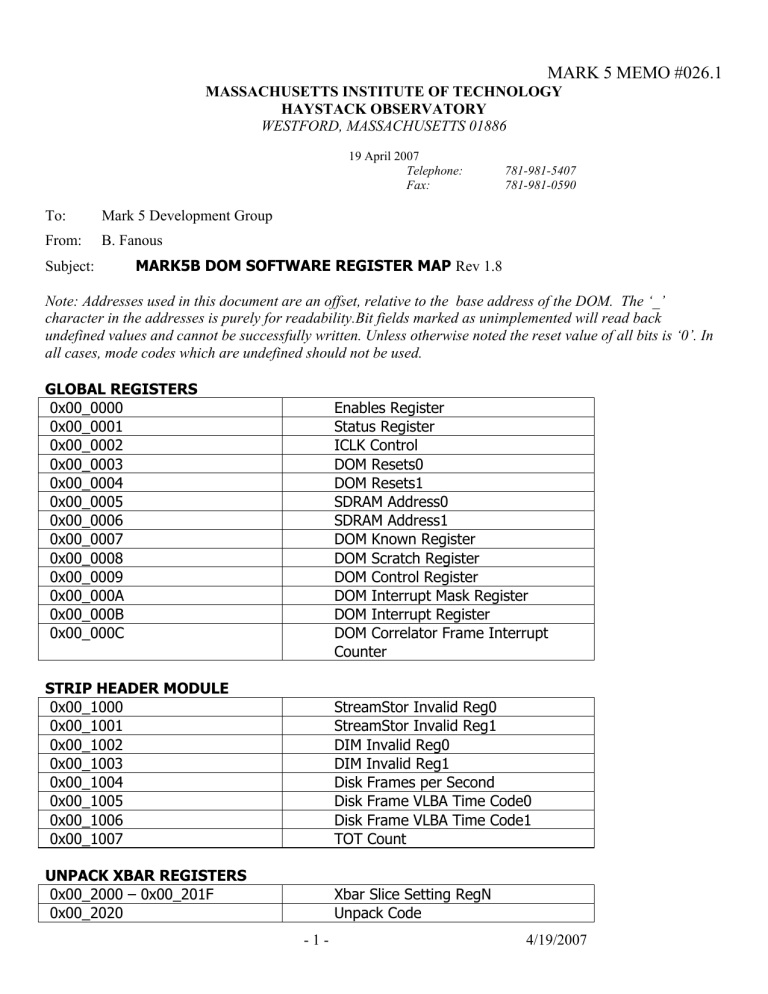
MARK 5 MEMO #026.1 MASSACHUSETTS INSTITUTE OF TECHNOLOGY HAYSTACK OBSERVATORY WESTFORD, MASSACHUSETTS 01886 19 April 2007 Telephone: Fax: To: Mark 5 Development Group From: B. Fanous Subject: 781-981-5407 781-981-0590 MARK5B DOM SOFTWARE REGISTER MAP Rev 1.8 Note: Addresses used in this document are an offset, relative to the base address of the DOM. The ‘_’ character in the addresses is purely for readability.Bit fields marked as unimplemented will read back undefined values and cannot be successfully written. Unless otherwise noted the reset value of all bits is ‘0’. In all cases, mode codes which are undefined should not be used. GLOBAL REGISTERS 0x00_0000 0x00_0001 0x00_0002 0x00_0003 0x00_0004 0x00_0005 0x00_0006 0x00_0007 0x00_0008 0x00_0009 0x00_000A 0x00_000B 0x00_000C Enables Register Status Register ICLK Control DOM Resets0 DOM Resets1 SDRAM Address0 SDRAM Address1 DOM Known Register DOM Scratch Register DOM Control Register DOM Interrupt Mask Register DOM Interrupt Register DOM Correlator Frame Interrupt Counter STRIP HEADER MODULE 0x00_1000 0x00_1001 0x00_1002 0x00_1003 0x00_1004 0x00_1005 0x00_1006 0x00_1007 StreamStor Invalid Reg0 StreamStor Invalid Reg1 DIM Invalid Reg0 DIM Invalid Reg1 Disk Frames per Second Disk Frame VLBA Time Code0 Disk Frame VLBA Time Code1 TOT Count UNPACK XBAR REGISTERS 0x00_2000 – 0x00_201F 0x00_2020 Xbar Slice Setting RegN Unpack Code -1- 4/19/2007 CORRELATOR FRAME HEADER RAM BANK 0x00_3000 – 0x00_30EF Correlator Frame Header RAM Bank A 0x00_3100 – 0x00_31EF Correlator Frame Header RAM Bank B DELAY GENERATOR 0x00_4000 0x00_4001 0x00_4002 0x00_4003 Delay Delay Delay Delay VSI OUTPUT MODULE 0x00_5000 VSI Output Configuration Register TIMING SUBSYSTEM 0x00_6000 0x00_6001 RCLK PPS Rate Register System PPS Suppress Register STATION UNIT BOCF GENERATOR 0x00_7000 0x00_7001 Correlator Frame Length Reg0 Correlator Frame Length Reg1 Station Unit Output Module 0x00_8000 SU Output Configuration Register Test Vector Receiver Module 0x00_9000 0x00_9001 0x00_9002 0x00_9003 0x00_9004 TVR TVR TVR TVR TVR Error Reg0 Error Reg1 Rate Reg0 Rate Reg1 Sum Reg0 Sum Reg1 Bit to Sum Reg Bias Reg0 Bias Reg1 The addresses above are internal to the DOM and are really 16-bit register locations. Though the addresses above increment by 1 between locations, this may not be so in the operating system, which typically increments a 16-bit register address by 2. However, the least significant bit from the PCI bus is dropped in making these internal addresses, so while the operating system addresses would increase by 2, the internal addresses will only increment by 1.One way of handling this address space is as an array of shorts in C with array location 0 at the DOM base address. Then let the operating system take care of the incrementing. NOTE: Phase Calibration Tone Extraction and State Count system are located between 0x00_A000 and 0x00_A9FF in the DOM, if implemented (see DOM Known Register). -2- 4/19/2007 DOM REGISTER DESCRIPTIONS GLOBAL REGISTERS Address 0x00_0000: Enables Register Enables the various blocks within the DOM. Bit 0 1 2 Type R/W R/W R/W Name fpdp_xface_en strip_header_en unpack_xbar_en 3 4 5 6 7 R/W R/W R/W R/W R/W xbar_ram_en sdram_arbiter_en sdram_core_en sdram_rcvr_en cfhr_en 8 9 10 11 12 13 14 15 R/W R/W R/W R/W R/W R/W R/W R delay_gen_en vsio_en suo_en timing_en bocf_gen_en tvg_en tvr_en 1 Description Enables the FPDP interface Enables the “strip header” module Enables the unpack-xbar module. Also Phase Cal enable if implemented. Enables the post-xbar RAM Enables the SDRAM arbiter Enables the SDRAM core functions Enables the SDRAM data receiver module Enables the Correlator Frame Header RAM module Enables the Delay Generator module Enables the VSI output module Enables the Station Unit output module Enables the Timing subsystem Enables the BOCF generation Enables the Test Vector Generator Enables the Test Vector Receiver -3- 4/19/2007 Address 0x00_0001: Status Register Provides some status of the DOM. Bit 0 Type R Name header_err 1 R DCM0 2 R DCM1 3 R sdram_clk_stopped 7-4 8 R R sdram_init_done 10-9 R sdram_fill 11 15-12 Bit 7-0 8 9 10 R R Type R/W R/W R/W R/W sdram_buffer_empty zero Name ICLK_data[7-0] ICLK_freq_update ICLK_rst ICLK_wl_clk Description Indicates a disk frame header error has occurred. Cleared by reseting the DOM. Indicates SDRAM DCM0 (board clock) has locked. Indicates SDRAM DCM1 (divided clock) has locked. Indicates that the SDRAM clk input has stopped. DOM should be reset. 0 Indicates the SDRAM has completed its initialization. 63999456 samples in buffer at end of init. 00 – SDRAM buffer is 0% - 25% full. 01 – SDRAM buffer is 25% - 50% full. 01 – SDRAM buffer is 50% - 75% full. 11 – SDRAM buffer is 75% - 100% full. Indicates the SDRAM buffer is empty. tied to 0 Description Internal clock data bits Internal clock frequency update Internal clock reset. Internal clock control clock -4- 4/19/2007 Address 0x00_0002: ICLK Control Control bits for the board “internal” clock. See data sheet for AD9850 clock generator. Address 0x00_0003: DOM Resets0 Resets for some DOM blocks. Bit 0 1 2 3 4 Type R/W R/W R/W R/W R/W Name fpdp_xface_rst fpdp_fifo_rst strip_header_rst sh_fifo_rst unpack_xbar_rst 5 6 7 8 9 10 11 12 13 14 Bit 0 1 2 R/W R/W R/W R/W R/W R/W R/W R/W R/W R/W Type R/W R/W R/W xbar_ram_rst cfdr_rst cfhr_rst delay_gen_rst vsio_rst suo_rst timing_rst bocf_gen_rst tvg_rst tvr_rst Name sdram_xface_rst dcm_rst fpdp_dcm_rst Bit 4-0 Type R/W Name sdram_addr[4-0] 11-6 R/W sdram_addr[11-6] 15-12 R/W sdram_addr[15-12] Description FPDP interface reset. FPDP receive FIFO reset. Strip Header module reset Post-Strip Header FIFO reset Unpack-Xbar reset. Also Phase Cal Reset (if implemented) Post-Xbar RAM module reset Correlator Frame Data RAM reset Correlator Frame Header RAM reset Delay Generator reset VSI Output module reset. Station Unit Output reset. Timing subsystem reset. BOCF generator reset. Test Vector Generator reset. Test Vector Receiver reset. Description Resets the entire SDRAM control interface. Resets the SDRAM clocking subsystem. Resets the FPDP DCM. Description SDRAM starting read address. Corresponds to offset in sdram_rcvr’s receive FIFO. SDRAM starting read address. Corresponds to SDRAM column address. SDRAM starting read address. Corresponds to lower 4 bits of SDRAM row address. -5- 4/19/2007 Address 0x00_0004: DOM Resets1 Resets for some DOM blocks. Address 0x00_0005: SDRA M Address0 Least significant bits of starting SDRAM read address used at next BOCF/VSI delay change. Address 0x00_0006: SDRAM Address1 Most significant bits of starting SDRAM read address used at next BOCF/VSI delay change. Bit 7-0 Type R/W Name sdram_addr[23-16] 9-8 R/W sdram_addr[25-24] Description SDRAM starting read address. Corresponds to upper 8 bits of SDRAM row address. SDRAM starting read address. Corresponds to SDRAM bank address. Register A read only known value containing configuration information. Bit Type Name Description 15-8 R known_val_reg[15-8] Value = 0x5B 7 R known_val_reg[7] 1 if DIM, 0 if DOM 6 R known_val_reg[6] 1 if phase cal is implemented 5-0 R known_val_reg[5-0] Revision Code (DIM & DOM may differ) Register A read/write scratch register for software. Bit 15-0 Type R/W Name scratch_reg Description Scratch register. -6- 4/19/2007 Address 0x00_0007: DOM Known Address 0x00_0008: DOM Scratch Address 0x00_0009: DOM Control Register Control register for some DOM global functionality. Bit Type Name Description 1-0 R/W back_end_mode[1-0] 2 R/W rclk_tristate_en 4-3 R/W qspare[2 -1] 5 R/W dpsclk_source 7-6 R/W sw_led0 Controls the color of software LED0 00 – LED is off. 01 – LED is red. 10 – LED is green. 11 – LED is blue. 9-8 R/W sw_led1 Bit 0 1 2 3 4 5 Type R/W R/W R/W R/W R/W R/W Name TOT_IM DOM1PPS_IM CF_IM New_TVR_Sums_IM ROT1PPS_IM PC_IM Controls the color of software LED1 00 – LED is off. 01 – LED is red. 10 – LED is green. 11 – LED is blue. Description Mask for TOT (Taken on Tick) interrupt. Mask for DOM1PPS interrupt. Mask for Correlator Frame interrupt. Mask for New_TVR_Sum interrupt Mask for ROT1PPS interrupt. Mask for Phase Cal interrupt (if implemented). Selects DOM mode. 00 – Station Unit 01 – VSI output 10 – TVG 11 - TVR Tristates the RCLK output. Resets to ‘1’. Software controllable qspare bits. qspare(2) = RESET# qspare(1) = DAV# to the serial links in SU mode. Indicates source of dpsclk 0 - Use VSI DSPCLK connector 1 – Use “internal” clock on board -7- 4/19/2007 Address 0x00_000A : DOM Interrupt Mask Register Interru pt Mask Register. A ‘1’ written to a bit enables that interrupt. Address 0x00_000B: DOM Interrupt Register Interrupt Register. Register is cleared on a read. Bit 0 Type INT Name TOT_INT 1 2 INT INT DOM1PPS_INT CF_INT 3 INT New_TVR_Sums_INT 4 INT ROT1PPS_INT 5 INT PC_INT Bit 15-0 Type R Name cf_cnt Description TOT (Taken on Tick) interrupt. Marks reading of TOT bit from disk. DOM1PPS interrupt. Marks DPS1PPS ticks Correlator Frame interrupt. Marks start of a new BOCF. New_TVR_Sum interrupt. Indicates a new error weight and DC bias has been calculated by the TVR. ROT1PPS interrupt. Marks system 1PPS (equivalent to ROT1PPS signal in VSI mode). Phase Calibration/State Count interrupt , if implemented. Description Increments from 0 with each BOCF. Rolls over at fullscale. -8- 4/19/2007 Address 0x00_000C: DOM Correlator Frame Interrupt Counter Counts the number of BOCFs since bocf_gen is first enabled. STRIP HEADER MODULE Address 0x00_1000: StreamStor Invalid Reg0 Lower half of the data word which indicates invalid data as marked by the SteamStor system. Resets to 0x55. Bit 15-0 Type R/W Name ssi[15-0] Description StreamStor invalid word, lower half Address 0x00_1001: StreamStor Invalid Reg1 Upper half of the data word which indicates invalid data as marked by the SteamStor system. Resets to 0xAA. Bit 15-0 Type R/W Name ssi[31-16] Description StreamStor invalid word, upper half Address 0x00_1002: DIM Invalid Reg0 Lower half of the data word which indicates invalid data as marked by the DIM. Can be the same as the StreamStor Invalid Reg0. Resets to 0x33. Bit 15-0 Type R/W Name dimi[15-0] Description DIM invalid word, lower half Address 0x00_1003: DIM Invalid Reg1 Upper half of the data word which indicates invalid data as marked by the DIM. Can be the same as StreamStor Invalid Reg1. Resets to 0xCC. Bit 15-0 Type R/W Name dimi[31-16] Description DIM invalid word, upper half Address 0x00_1004: Disk Frames per Second Number of Disk Frames in 1 second of recorded time. This number is 1’s based (i.e. a value of 100 indicates 100 disk frames per second, as opposed to a 0-based number which would indicate 101 frames per second.). Resets to 0x100. Bit 14-0 Type R Name frames_per_sec[14-0] Description Disk Frames per second. -9- 4/19/2007 Address 0x00_1005: Disk Frame VLBA Time Code0 Contains the 16 lsbs of the VLBA time code (word 1 of the Disk Frame Header) captured when the DOM’s internal frame counter rolls over (frames_per_sec disk frames have been read off the disk). It is possible that this word could be marked invalid by the StreamStor. Bit 15-0 Type R Name df_tc[15-0] Description Disk Frame Time Code. Address 0x00_1006: Disk Frame VLBA Time Code1 Contains the 16 msbs of the VLBA time code (word 1 of the Disk Frame Header) captured when the DOM’s internal frame counter rolls over (frames_per_sec disk frames have been read off the disk). It is possible that this word could be marked invalid by the StreamStor. Bit Type Name Description 15-0 R df_tc[31-16] Disk Frame Time Code. Address 0x00_1007: TOT Count Set to 0 on reset, this counter increments every time the internal disk frame counter rolls over (i.e. every time frames_per_sec number of disk frames have been taken off the FPDP bus). The value rolls over at full scale. This is equivalent to the number of TOT_INTs which have occurred since FPDP accesses began, provided that the interrupt was enabled the entire time. Bit 15-0 Type R Name tot_cnt[15-0] Description TOT (Taken on Tick) Count - 10 - 4/19/2007 UNPACK XBAR REGISTERS Address 0x00_2000 – 0x00_201F: Xbar Slice Setting RegN These 32 5-bit registers control the crossbar (xbar) setting. The value should be the source mapping for the Nth bit of the Xbar output.. The xbar_slice_src value is the binary unsigned number from 0 to 31 which is the bit index of the input word to be mapped to output bit N. That is: xbar_output(N) <= Xbar_input(xbar_slice_src); Bit 4-0 Type R/W Name xbar_sliceN_src[4-0] Description Bit index of Xbar input to be the source of Xbar output word bit N. Resets to N (i.e. Xbar is a thru). Address 0x00_2020 : Unpack Code Contains the Unpack Code indicating the Data Array Format (active bit streams per 32 bit word). An M bit stream data word format means that in a 32 bit StreamStor word there are 32/M actual data words each M bits long. Bit 2-0 Type R/W Name unpack_code[2-0] 14-3 15 R/W unimplemented one_bit_samples Description Unpack Code 000 – 32 bit stream data word format 001 – 16 bit stream data word format 010 – 8 bit stream data word format 011 –4 bit stream data word format 100 – 2 bit stream data word format 101 – 1 bit stream data word format unimplemented Should be set if data encoding on disk uses onebit samples. Cleared if using two-bit samples. - 11 - 4/19/2007 CORRELATOR FRAME HEADER RAM BANK Address 0x00_3000 – 0x00_30EF: Correlator Frame Header RAM Bank A The Correlator Frame Header RAM (CFHR) Bank A hold the 240 16-bit correlator frame header words for the 1st, 3rd, 5th, … correlator frames. This should be pre-loaded prior to station unit output being triggered. Each of the 16 bits in a RAM location maps to a magnitude output bit stream. This RAM should be updated after CF_INTs 2,4,6,8,... . Bit 15-0 Type R/W Name cfhrA[15-0] Description Correlator Frame Header words. Address 0x00_3100 – 0x00_31EF: Correlator Frame Header RAM Bank B The Correlator Frame Header RAM (CFHR) Bank B hold the 240 16-bit correlator frame header words for the 2nd, 4th, 6th, … correlator frames. This should be pre-loaded prior to station unit output being triggered. Each of the 16 bits in a RAM location maps to a magnitude output bit stream. This RAM should be updated after CF_INTs 3,5,7… . Bit 15-0 Type R/W Name cfhrB[15-0] Description Correlator Frame Header words. - 12 - 4/19/2007 DELAY GENERATOR Address 0x00_4000 : Delay Error Reg0 This register is written with the lower half of the delay error (a 32-bit unsigned number). It should be written to prior to output triggering and after every CF_INT. Resets to 0x0000. Bit 15-0 Type R/W Name del_err[15-0] Description LSBs of the 32-bit unsigned number indicating the delay error associated with the next Correlator Frame. Address 0x00_4001 : Delay Error Reg1 This register is written with the upper half of the delay error (a 32-bit unsigned number). It should be written to prior to output triggering and after every CF_INT. Resets to 0xFFF0 Bit 15-0 Type R/W Name del_err[31-16] Description MSBs of the 32-bit unsigned number indicating the delay error associated with the next Correlator Frame. Address 0x00_4002 : Delay Rate Reg0 This register is written with the lower 16 bits of the delay rate (an 18-bit unsigned number). It should be written to prior to output triggering and after every CF_INT. Resets to 0xFFFF. Bit 15-0 Type R/W Name del_rate[15-0] Description LSBs of the 32-bit unsigned number indicating the delay rate associated with the next Correlator Frame. - 13 - 4/19/2007 Address 0x00_4003 : Delay Rate Reg1 This register is written with the upper 2 bits of the delay rate (an 18-bit unsigned number). It should be written to prior to output triggering and after every CF_INT. This also contains the delay generator mode bit which is also updated every CF_INT. Resets to 0x0003. Bit 1-0 14-2 15 Type R/W Name del_rate[17-16] R/W unimplemented del_gen_mode Description MSBs of the 18-bit unsigned number indicating the delay rate associated with the next Correlator Frame. unimplemented Delay Generator Mode Bit 0 – Repeat output of last data word on Delay Adder Carry Out. 1 – Skip output of next data word on Delay Adder Carry Out. - 14 - 4/19/2007 VSI OUTPUT MODULE Address 0x00_5000 : VSI Output Configuration Register Configures the VSI Output module. Bit 2-0 14-3 15 Type R/W Name vsi_prescl_code[2-0] R/W unimplemented vsio_run Description Controls the baud rate of the data output in VSI mode relative to the RCLOCK frequency. 000 – Output data baud = RCLK freq. 001 - Output data baud = RCLK freq/2 010 – Output data baud = RCLK freq/4 011 – Output data baud = RCLK freq/8 100 - Output data baud = RCLK freq/16 unimplemented VSI Output Run bit. 1 – start output on next unsuppressed system 1PPS. 0 – stop output on next unsuppressed system 1PPS. This is useful for back-to-back scans without emptying the RAM buffer. - 15 - 4/19/2007 TIMING SUBSYSTEM Address 0x00_6000 : RCLK PPS Rate Register Configures the RCLOCK and the system 1PPS. Bit 2-0 Type R/W 5-3 6 R/W Name rclk_rate_code[2-0] Description Controls the division of the dpsclk (or board “internal” clock) in the generation of rclk. 000 – RCLK freq = DPSCLK freq 001 – RCLK freq = DPSCLK freq/2 010 – RCLK freq = DPSCLK freq/4 011 – RCLK freq = DPSCLK freq/8 100 – RCLK freq = DPSCLK freq/16 PPS_div_code[2-0] Controls how many DPSCLK cycles per 1PPS. 000 – 128 million DPSCLKs per PPS. 001 – 64 million DPSCLKs per PPS 010 – 32 million DPSCLKs per PPS 011 – 16 million DPSCLKs per PPS 100 – 8 million DPSCLKs per PPS 101 – 4 million DPSCLKs per PPS 110 – 2 million DPSCLKs per PPS 111 – 100 DPSCLKs per PPS (for testing only). Controls the source of the 1PPS start trigger. 0 – the DPS1PPS will trigger the start of the PPS divider/generator. 1 – enabling the timing subsystem will trigger the start of the PPS divider/generator (for use when there is no DPS1PPS). use_internal_pps - 16 - 4/19/2007 Address 0x00_6001 : System PPS Suppress Register Controls the suppression of the DOM internal 1PPS pulse which is used to trigger several blocks. An unsuppressed 1PPS will load a new SDRAM read starting address in VSI mode (to change the delay), and begin output from the VSI Output module or SU Output module. In TVG or TVR mode an unsuppressed 1PPS will begin test vector processing. Bit 0 Type R/W Name suppress_pps Description 1 – Suppress generation of internal 1PPS. 0 – Allow internal 1PPS. Resets to 1. - 17 - 4/19/2007 STATION UNIT BOCF GENERATOR Address 0x00_7000 : Correlator Frame Length Reg0 Lower 16 bits of the29-bit, 0-based word which indicates the correlator frame data payload length in Station Unit mode. Length is measured in RCLKs Bit Type Name Description 15-0 R/W cf_payload_len[15-0] LSBs of number of RCLKs (24-bits wide) in a CF Address data payload. 0x00_7001 : Correlator Frame Length Reg1 Upper 16 bits of the 29-bit, 0-based word which indicates the correlator frame data payload length in Station Unit mode. This also contains the BOCF length code. Bit Type Name Description 12-0 R/W cf_payload_len[31-16] MSBs of number of RCLKs (29-bits wide) in a CF data payload. 15-13 R/W bocf_code[2-0] Indicates the length of a BOCF 000 – BOCF is 240 RCLK cycles 001 – BOCF is 480 RCLK cycles 010 – BOCF is 960 RCLK cycles 011 – BOCF is 1920 RCLK cycles 100 – BOCF is 3840 RCLK cycles - 18 - 4/19/2007 STATION UNIT OUTPUT MODULE Address 0x00_8000 : SU Output Configuration Register Configures the SU Output module. Bit 3-0 14-4 15 Type R/W Name suo_prescl[3-0] R/W unimplemented suo_run Description suo_prescl is an unsigned, 4-bit terminal count for a zero based counter in the station unti output. This counter increments every RCLK cycle and when it reaches suo_prescl, the counter rolls over to zero and a new data word is placed on the output pins. This is similar to vsi_prescl_code. The only valid values are 0000, 0001, 0011, 0111, or 1111. unimplemented Similar to the vsio_run bit: 1 – start Station Unit output at next BOCF. 0 – stop Staiton Unit output at next BOCF. - 19 - 4/19/2007 TEST VECTOR RECEIVER MODULE Address 0x00_9000 : TVR Sum Reg0 Lower 16 bits of the 32-bit number indicating the error weight (number of incorrect bits) occurring on the bit indicated by tvr_bit2sum in 1 TOT second. Bit 15-0 Type R Name tvr_sum[15-0] Description Lower 16 bits of TVR error weight sum. : Address 0x00_9001 TVR Sum Reg1 Upper 16 bits of the 32-bit number indicating the error weight (number of incorrect bits) occurring on the bit indicated by tvr_bit2sum in 1 TOT second. Bit 15-0 : Type R Name tvr_sum[31-16] Description Upper 16 bits of TVR error weight sum. Address 0x00_9002 TVR Bit to Sum Reg Index of the data bit to process in the TVR. Can be changed every NEW_TVR_SUM_INT. Bit 4-0 Type R Name tvr_bit2sum[4-0] Description Index in binary (0 -31) of data bit to process (calculate error totals and DC bias) in the TVR. : Address 0x00_9003 TVR Bias Reg0 Lower 16 bits of the 32-bit, 2’s complement number indicating the DC Bias of the bit indicated by tvr_bit2sum in 1 TOT second. Bit 15-0 Type R Name tvr_bias[15-0] Description Lower 16 bits of TVR dc bias. Address 0x00_9004 : TVR Bias Reg1 Upper 16 bits of the 32-bit, 2’s complement number indicating the DC Bias of the bit indicated by tvr_bit2sum in 1 TOT second. Bit 15-0 Type R Name tvr_bias[31-16] Description Upper 16 bits of TVR dc bias. - 20 - 4/19/2007


