Trend of Energy Saving in Electronic Devices for Research and Development (
advertisement
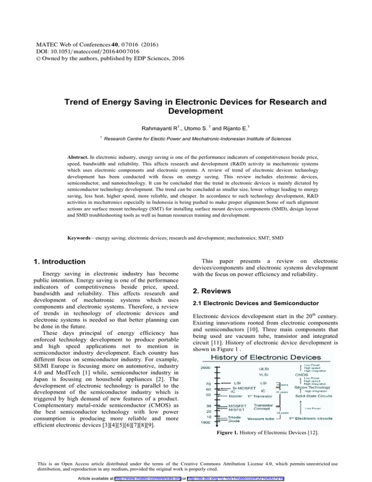
MATEC Web of Conferences 4 0, 0 7 016 (2016 ) DOI: 10.1051/ m atecconf/ 2016 4 0 0 7 016 C Owned by the authors, published by EDP Sciences, 2016 Trend of Energy Saving in Electronic Devices for Research and Development 1 1 Rahmayanti R ., Utomo S. and Rijanto E. 1 1 Research Centre for Electic Power and Mechatronic-Indonesian Institute of Sciences Abstract. In electronic industry, energy saving is one of the performance indicators of competitiveness beside price, speed, bandwidth and reliability. This affects research and development (R&D) activity in mechatronic systems which uses electronic components and electronic systems. A review of trend of electronic devices technology development has been conducted with focus on energy saving. This review includes electronic devices, semiconductor, and nanotechnology. It can be concluded that the trend in electronic devices is mainly dictated by semiconductor technology development. The trend can be concluded as smaller size, lower voltage leading to energy saving, less heat, higher speed, more reliable, and cheaper. In accordance to such technology development, R&D activities in mechatronics especially in Indonesia is being pushed to make proper alignment.Some of such alignment actions are surface mount technology (SMT) for installing surface mount devices components (SMD), design layout and SMD troubleshooting tools as well as human resources training and development. Keywords—energy saving; electronic devices; research and development; mechatronics; SMT; SMD 1. Introduction Energy saving in electronic industry has become public intention. Energy saving is one of the performance indicators of competitiveness beside price, speed, bandwidth and reliability. This affects research and development of mechatronic systems which uses components and electronic systems. Therefore, a review of trends in technology of electronic devices and electronic systems is needed so that better planning can be done in the future. These days principal of energy efficiency has enforced technology development to produce portable and high speed applications not to mention in semiconductor industry development. Each country has different focus on semiconductor industry. For example, SEMI Europe is focusing more on automotive, industry 4.0 and MedTech [1] while, semiconductor industry in Japan is focusing on household appliances [2]. The development of electronic technology is parallel to the development of the semiconductor industry which is triggered by high demand of new features of a product. Complementary metal-oxide semiconductor (CMOS) as the best semiconductor technology with low power consumption is producing more reliable and more efficient electronic devices [3][4][5][6][7][8][9]. This paper presents a review on electronic devices/components and electronic systems development with the focus on power efficiency and reliability. 2. Reviews 2.1 Electronic Devices and Semiconductor Electronic devices development start in the 20th century. Existing innovations rooted from electronic components and semiconductors [10]. Three main components that being used are vacuum tube, transistor and integrated circuit [11]. History of electronic device development is shown in Figure 1 . Figure 1. History of Electronic Devices [12]. This is an Open Access article distributed under the terms of the Creative Commons Attribution License 4.0, which permits XQUHVWULFWHGXVH distribution, and reproduction in any medium, provided the original work is properly cited. Article available at http://www.matec-conferences.org or http://dx.doi.org/10.1051/matecconf/20164007016 MATEC Web of Conferences In the era of vacuum tube, the size of a component is bigger than 1 mm. Vacuum tube was replaced by small dimension transistor that has low voltage. Most used semiconductor component are diode, transistor, fieldeffect transistor (FET), junction gate field-effect transistor (JFET), The metal-oxide-semiconductor fieldeffect transistor (MOSFET) and integrated circuit (IC). Electronic circuits in which the components are placed on printed circuit board (PCB) are called discret circuit. Electronic circuits in which the components are printed inside a silicon chip can be called as IC. To give background on how electronic device develops, generally in Table 1 is illustrated the comparison of electronic circuit design using integrated circuit. Table 1. Discrete vs integrated circuit design.[13] Activity / Item Component Accuracy Breadboarding Fabrication Physical Implementation Simulation Testing Computer Aided Design (CAD) Components Discrete Well known Yes Independent PC layout Model parameters well know Generally complete testing is possible Schematic capture, Simulation, PC Board Layout All possible Integrated Poor absolute accuracies No (kit Parts) Very dependent Layout, verification and extraction nanometer. Nowadays, miniaturization technology of semiconductor by using nanotechnology [16] has been implemented in countries dominating global semiconductor industry, such as Europe, Japan, South Korea, Taiwan and United States [17]. 2.4 Observation of Electronic Development in Indonesia Devices The development of electronic technology in Indonesia is parallel to the demand of users in the field of research and development (R&D). One of popular technology development is in the field of Robotic and Mechatronic. Figure 2 is an example of the implementation of IC in microcontroller. From left to right are shown the shift of microcontroller board with chips from ATMEL, the changes is not just from the dimension but also from its performance, size of the bit, working frequency and also features, as illustrated in Table 2. Model parameters vary widely Must be considered before design Figure 2. Microcontroller board used for R&D in robotic and mechatronics Schematic Capture, Simulation, extraction, layout and routing Active devices, capacitors, and resistor Table 2. Example of Microcontroller Trend Feature Technology Chip size Stated in [13] we know that compared to discret circuit, IC consumes lower, faster and better for signal related application. Generally, packaging standard of semiconductors is based on Joint Electron Device Engineering Council (JEDEC) and Japan Electronic and Information Technology Industries Association (JEITA), whereas some companies use their own. Some purpose based semiconductor packages are available in [14]. Semiconductor packaging available nowadays is also for surface mount package. I/O RAM Flash Memory Max. Clock frequency Max Operating Voltage Power Consumption 2.2 Semiconductor Industry The International Technology Roadmap for Semiconductor (ITRS) is a document produced by the group of world semiconductor companies from Europe, Japan, South Korea, Taiwan and United States. ITRS was designed and shown as technology rating without considering the individual commercial product [15]. 2.3 Nanotechnology Left 8 Max.14 x52.5 32 2 32 Middle 8 Max. 7x7 Units Bit mm 20 2 32 Right 32 Max.20 x20 68 96 512 16 16 84 MHz 5.5 5 3.3 V At 1 MHz, 3 V, 25°C Active Mode : 1.1 mA Powerdown Mode : < 1 μA At 1 MHz, 1.8 V, 25°C Active Mode : 0.2 mA Powerdown Mode : 0.1 μA Low Power Mode Sleep and Backup Mode : 2.5 μA pin KBytes KBytes Figure 3 is motor controller circuit in which microcontroller, power supply, driver circuit for motor, signal conditioning ciruit for sensors are fixed in a PCB. This exposes an example of semiconductor implementation of electronic devices. Nanotechnology is a design and a production by implementing a system or a device in the scale of 07016-p.2 ICMES 2015 Figure 3. Motor controller including microcontroller, power supply, motor driver, and signal conditioning circuits Table 3 has the completeness of features from motor controller circution in Figure 3. Table 3. Motor Controller Feature Power Circuit IC Type Max Current Sensor Non SMD Circuit Motor Driver (Left) 2 DC Voltage Regulator 8 Bit Microcontroller Dual Full-Bridge Driver Stepper Motor Controller Max 232 4A SMD Circuit Motor Driver (Right) DC Voltage Regulator 3-Phase power converter ECU 3-Phase Motor Drive 8 Bit Microcontroller Op-Amp Passivated Bridge Rectifier > 10 A No Sensor Hall Sensing Figure 4. Transistor Development based on Law’s of Moore [1] From Figure 4 it can be seen data of the amount of transistor in a chip and the production cost of a transistor annually. Based on that data, the cost per 1000 transistors in 2015 is 0.0003$ cheaper than the cost in 1971 that was 150$. In Figure 5 it is illustrated Intel's revolutionary 22nm transistor technology by Mark Bohr and Kaizad Mistry. Clearly can be seen in Figure 3, nowadays the dimension of components is smaller. Surface mount device (SMD) component used in Figure 2 and Figure 3 while, the process of installing SMD components on PCB is using surface mount technology (SMT). One of assembling techniques being used is solder paste [18]. SMD components dimension is smaller than discret components. The design of small dimension electronic devices can be done because of this SMT technology. 3. Discussion The trend of semiconductor technology for the producer takes place in term of product design, architecture, algorithm, software and evolution of life cycle [19]. The development of semiconductor is driven by the development of IC design. Design strategy of IC implemented nowadays is to reduce the complexity, increase productivity, and the guarantee of well-working product [14]. Semiconductor industry in United States is represented by SIA (Semiconductor Industry Association). Based on annual report of SIA in 2005 that there are more transistors are produced with cost lower than a grain rice [20]. A history analyst, Gordon Moore, estimates that the amount of transistor in a chip will rise exponentially [21-24]. In Figure 4 it is shown the development of transistor inside a chip. Figure 5. Intel’s revolutionary 22nm Transistor Technology [25] Three gate transistors when operated in low voltage will raise the performance as explained by Bohr [25]. Meanwhile in Figure 6 is illustrated the operating voltage of IC year by year. Figure 6. Energy saving performance of IC’s year by year [26][10] It can be seen clearly that in the 90’s working voltage less than 5 volt has been introduced and micro technology was also being used. In the beginning of 2000, nanotechnology was started to be introduced, when the dimension of IC in the scale of nano then the working voltage was reduced to 1 Volt. The performance of IC is increasing parallel to its dimension. With the existence of 07016-p.3 MATEC Web of Conferences miniaturization, power consumption is lessen [27]. This implies larger energy saving as shown by Equation (1) [28]. P = ACV2f + VIleak (1) Where A is procentage of gate switching, C capacitance, V represents supply voltage, F = operating frequency, and Ileak for leakage current. Figure 7 displays the document of ITRS about the development of semiconductor from 2002 to 2014. Figure 7. International Semiconductors [12] Technology Roadmap for In the ITRS document it can be seen the development of semiconductor year by year and can be concluded that the future development of semiconductor will be low voltage, low power dissipation, higher working frequency, small dimension and packaging [29-30], the use of nanotechnology and more input/output (I/O) is available [31]. 3.1 The Present and The Future Small dimension allows more transistors to be packed into one chip [14]. This endorses semiconductor industry to adopt innovation miniaturization leading to nanotechnology. Based on Moore's law, miniaturization is approaching the limit and is now already to be used in nanoscale dimension. One way to overcome this limit is to combine the chip technology with a packaging technology that can accumulate chips into 3D integrated chips [22] [32-33]. When the dimension of IC became smaller electrical resistance, power density and thermal of the chips increase [34]. To overcame this case, normally IC is made dependent on the purpose and the workload [35]. 3.2 Case Study The limit of supporting components and mounting tools for low power consumption devices are current R & D obstacle. For example, in the process of R&D using brushless motor or other kinds of motor, the power supply used has 5 V of power, while microcontrollers that have full features needs 3.3 V. In order to solve such a problem, additional electronic circuits are needed to convert the voltage, illustrated in Figure 8. Figure 8. Solved problem of speed control brushless DC motor 4. Conclusion Nowadays semiconductor development is the miniaturization of the dimension by using newest technology towards nanoelectronic < 50 nm. The technology trend can be shortened as smaller size, lower voltage, energy saving, less heat, higher speed, more reliable, and cheaper. Semiconductor low voltage and low power semiconductor can be accommodated using pure DC sources. It is expected that smaller circuits can be used for bigger benefit. In Indonesia, R&D activities in mechatronics is being pushed to make proper alignment. Some of such alignment actions are SMT technology for installing SMD components, design layout and SMD troubleshooting tools. For this human resources training and development is crucial. Acknowledgement We would like to express our gratitude to the entire researchers in Research Centre for Electrical Power and Mechatronics, Indonesian Institute of Sciences. References 1. 2. 3. 4. 5. 6. 07016-p.4 Raithel, Stephan. Innovation Driven by Semiconductors. Retrieved from http://semi.org/en/node/56431. Last visited on July 2015. (2015).M. Ben Rabha, M.F. Boujmil, M. Saadoun, B. Bessaïs, Eur. Phys. J. Appl. Phys. (to be published) Nirmala, Junko. Rise and Fall of Japan’s ElectronicsSemiconductor Industry : Will India take lead?. Retrieved from http://www.financialexpress.com/article/industry/co mpanies/rise-and-fall-of-japans-electronicssemiconductor-industry-will-india-take-lead/45798/. Last visited on July 2015. (2015). Serdijn, W. A., Van Der Woerd, A. C., Van Roermund, A. H., & Davidse, J. Design principles for low-voltage low-power analog integrated circuits.Analog Integrated Circuits and Signal Processing, 8.1 (1995) : 115-120. Prodanov, Vladimir I., and Michael M. Green. "Design Techniques and Paradigms Toward Design of Low-Voltage CMOS Analog Circuits." Electrical Engineering (1997): 152. Marks, Tobin J., and Mark C. Hersam. "Materials science: Semiconductors grown large and thin." Nature 520.7549 (2015): 631-632. Harrison, R.R.; Charles, C., "A low-power low-noise CMOS amplifier for neural recording applications," ICMES 2015 7. 8. 9. 10. 11. 12. 13. 14. 15. 16. 17. 18. 19. 20. in Solid-State Circuits, IEEE Journal of , vol.38, no.6, pp.958-965, June 2003. Kim, Dae-Hyeong, et al. "Stretchable and foldable silicon integrated circuits."Science 320.5875 (2008): 507-511. Cevik, Ismail, et al. "An Ultra-Low Power CMOS Image Sensor with On-Chip Energy Harvesting and Power Management Capability." Sensors 15.3 (2015): 5531-5554. H. Soeleman, K. Roy and B. Paul, “Robust ultra-low power subthreshold DTMOS logic,” in ISLPED, pp. 25-30, 2000. Sicard, Etienne, and J. M. Dienot. "Issues in electromagnetic compatibility of integrated circuits: emission and susceptibility." Microelectronics reliability 45.9 (2005): 1277-1284. M. Ramdani, E. Sicard, A. Boyer, S. Ben Dhia, J. J. Whalen, T. Hubing, M. Coenen, and O. Wada, “The electromagnetic compatibility of integrated circuits—Past, present and future,” IEEE Trans. Electromagn. Compat., vol. 51, no. 1, pp. 78–100, Feb. 2009. Wang, Deli. Nanoelectronics [Presentation slide]. Retrieved from http://electronics.wesrch.com/paperdetails/pdf-EL1SE1F57NGHN-emergingnanoelectronic-devices-and-architectures#page1. Last visited on July 2015. (2010). Erkmen, B. Integrated Circuit Technology Overview [Presentation slide]. Retrieved from http://www.yarbis1.yildiz.edu.tr/web/userCourseMat erials/mnkurnaz_c1e2b7fb00efdea6fcc1da1f0b682f6 7.pdf. Last visited on July 2015. (2014). ______. Type of Semiconductor Packaging [Technical Reference]. Retrieved July 7, 2015, from RS Australia Electronics Centre: http://au.rsonline.com/web/generalDisplay.html?id=centre/eem _techref_semipack. (2009). Allan, A. 2008 ITRS ORTC [Public Conference Preparation]. Retrieved July 7, 2015, from International Technology Roadmap for Semiconductors: http://cseweb.ucsd.edu/classes/wi09/cse242a/itrs/OR TC.pdf¬¬.(2008). Peschot, Alexis, Chuang Qian, and Tsu-Jae King Liu. "Nanoelectromechanical Switches for Low-Power Digital Computing." Micromachines 6.8 (2015): 1046-1065. Bassett, Deborah R. "Taniguchi, Norio". In Guston, David H. Encyclopedia of nanoscience and society. London: SAGE. p. 747. ISBN 9781452266176. Retrieved 3 july 2015. (2010) Rahman, Mohd Nizam Ab, et al. "Reliability Study of Solder Paste Alloy for the Improvement of Solder Joint at Surface Mount Fine-Pitch Components."Materials 7.12 (2014): 7706-7721. Vidhya, M., & Kamalakannan, R.S. Implementation of MCC ADDER with low power dissipation based on spst. International Journal of Research Science & Management 2.5 (2015), :12-18. Bennett, Herbert S. "Will future measurement needs of the semiconductor industry be met?." JOURNAL 21. 22. 23. 24. 25. 26. 27. 28. 29. 30. 31. 32. 33. 34. 35. 07016-p.5 OF RESEARCH-NATIONAL INSTITUTE OF STANDARDS AND TECHNOLOGY 112.1 (2007): 25. Agenda, S. I. A. "Letter from the President 6 The Man Behind the Law 8 40 Years of Moore’s Law 10 Moore’s Law and the Emergence of the New Economy 16 About SIA 21." Liu, Yingxia, et al. "A metastable phase of tin in 3D integrated circuit solder microbumps." Scripta Materialia 102 (2015): 39-42. Huynh, Hai Au, et al. "Analysis of Power Transfer Efficiency of Standard Integrated Circuit Immunity Test Methods." International Journal of Antennas and Propagation 2015 (2015). Sarkar, Aveek. "Low Power, High Performance." EXCELLENCE IN ENGINEERING SIMULATION (2011): 26. Bohr, Mark, and Kaizad Mistry. "Intel’s revolutionary 22 nm transistor technology." Intel website (2011). "Research." Research. E3S Center for Energy Efficient Electronics Science, n.d. Web. 18 Sept. 2015. <http://www.e3s-center.org/research/>. Carlton, Ross M. "An overview of standards in electromagnetic compatibility for integrated circuits." Microelectronics journal 35.6 (2004): 487495. Kim, Nam Sung, et al. "Leakage current: Moore's law meets static power."computer 36.12 (2003): 6875. Kaware, U. W., Ms Anushri Garud, and Mr Shubham Deshmukh. "A DFT technique for MCM (Multi Chip Module) testing." nature 4.1 (2015). Schaller, Robert R. Technological innovation in the semiconductor industry: a case study of the International Technology Roadmap for Semiconductors (ITRS). Diss. George Mason University, 2004. Shanmugavel, Arvind. "Robust Design for Integrated Circuits." (2013).\ Deptuch, Grzegorz W., et al. "Results of tests of three-dimensionally integrated chips bonded to sensors." Nuclear Science, IEEE Transactions on 62.1 (2015): 349-358. Mei, Qinggao, et al. "An Efficient Transient ElectroThermal Simulation Framework for Power Integrated Circuits." (2015). Allec, Nicholas, et al. "ThermalScope: multi-scale thermal analysis for nanometer-scale integrated circuits." Computer-Aided Design, 2008. ICCAD 2008. IEEE/ACM International Conference on. IEEE, 2008. Joshi, Yogendra K. "An Efficient Approach for MULTI-SCALE Thermal Modeling of Integrated Circuits." Electronics Cooling Magazine Focused on Thermal Management TIMs Fans Heat Sinks CFD Software LEDsLighting. Electronics Cooling, 15 Sept. 2015. Web. 18 Sept. 2015. <http://www.electronics-cooling.com/2015/09/anefficient-approach-for-multi-scale-thermal-modelingof-integrated-circuits/>.
