Technical Article ICs SIMPLIFY THE DESIGN OF DIGITAL COMMUNICATIONS LINKS
advertisement
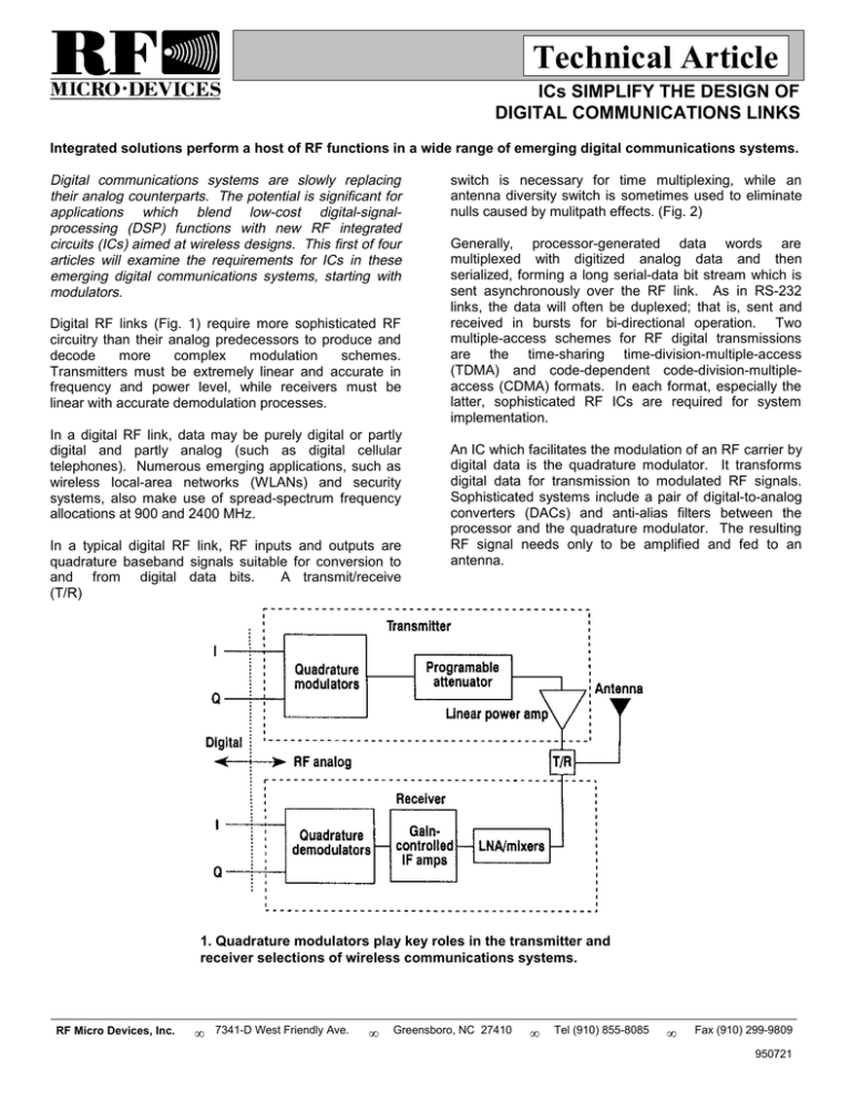
Technical Article ICs SIMPLIFY THE DESIGN OF DIGITAL COMMUNICATIONS LINKS Integrated solutions perform a host of RF functions in a wide range of emerging digital communications systems. Digital communications systems are slowly replacing their analog counterparts. The potential is significant for applications which blend low-cost digital-signalprocessing (DSP) functions with new RF integrated circuits (ICs) aimed at wireless designs. This first of four articles will examine the requirements for ICs in these emerging digital communications systems, starting with modulators. Digital RF links (Fig. 1) require more sophisticated RF circuitry than their analog predecessors to produce and decode more complex modulation schemes. Transmitters must be extremely linear and accurate in frequency and power level, while receivers must be linear with accurate demodulation processes. In a digital RF link, data may be purely digital or partly digital and partly analog (such as digital cellular telephones). Numerous emerging applications, such as wireless local-area networks (WLANs) and security systems, also make use of spread-spectrum frequency allocations at 900 and 2400 MHz. In a typical digital RF link, RF inputs and outputs are quadrature baseband signals suitable for conversion to and from digital data bits. A transmit/receive (T/R) switch is necessary for time multiplexing, while an antenna diversity switch is sometimes used to eliminate nulls caused by mulitpath effects. (Fig. 2) Generally, processor-generated data words are multiplexed with digitized analog data and then serialized, forming a long serial-data bit stream which is sent asynchronously over the RF link. As in RS-232 links, the data will often be duplexed; that is, sent and received in bursts for bi-directional operation. Two multiple-access schemes for RF digital transmissions are the time-sharing time-division-multiple-access (TDMA) and code-dependent code-division-multipleaccess (CDMA) formats. In each format, especially the latter, sophisticated RF ICs are required for system implementation. An IC which facilitates the modulation of an RF carrier by digital data is the quadrature modulator. It transforms digital data for transmission to modulated RF signals. Sophisticated systems include a pair of digital-to-analog converters (DACs) and anti-alias filters between the processor and the quadrature modulator. The resulting RF signal needs only to be amplified and fed to an antenna. 1. Quadrature modulators play key roles in the transmitter and receiver selections of wireless communications systems. RF Micro Devices, Inc. • 7341-D West Friendly Ave. • Greensboro, NC 27410 • Tel (910) 855-8085 • Fax (910) 299-9809 950721 Technical Article ICs SIMPLILFY THE DESIGN OF DIGITAL COMMUNICATIONS LINKS 2. In a typical RF data system, a high-speed switch selects between receiver and transmitter sections. Some systems may generate data with an applicationspecific integrated circuit (ASIC) and feed the digital data directly to the quadrature modulator. Spread-spectrum data transmitters are often implemented by convolving the data with the pseudo-random spreading sequence and applying digital signals directly to a quadrature modulator. In frequency-shift keying (FSK), a modulated frequency (ƒm) is added to a carrier frequency (ƒc) to represent a binary 1 or subtracted from the carrier for a binary 0. The carrier frequency is set by a crystal oscillator with a phase-locked loop (PLL) or a direct digital synthesizer (DDS). The processor typically controls the transmit and receive frequencies to minimize interference and maximize data reception. A simple FSK scheme involves application of the modulating signal to the PLL. Time-multiplexed FSK requires that the signal be ramped up and down in order to avoid spectral splatter from the instantaneous change of digital states. Similarly, the pan-European GSM system employs Gaussian- minimum-shift-keying (GMSK) modulation to conserve frequency spectrum. In this approach, a Gaussian filter smoothes the modulation signal; the system operates with partial responses with minimized bandwidth requirements and greatly-attenuated out-of-band sidelobes. The Gaussian filters are implemented digitally. The quadrature components of the modulating signal are digitally derived, converted to analog signals with DACs, and applied to a quadrature modulator. Unlike FSK, quadrature phase-shift keying (QPSK) permits the transmitted symbol to contain more than one bit of information, increasing the amount of data per frequency channel. QPSK is most-commonly generated by quadrature modulators. The quadrature modulator allows control of the phase and amplitude of the RF carrier. Frequency modulation (FM), phase modulation (PM), and/or amplitude modulation (AM) can be achieved by orthogonal modulation of the fixed carrier while generating low spurious products. The RF signal generated by the quadrature modulator can be expressed as: RF Micro Devices, Inc. • 7341-D West Friendly Ave. • Greensboro, NC 27410 • Tel (910) 855-8085 • Fax (910) 299-9809 950721 Technical Article ICs SIMPLILFY THE DESIGN OF DIGITAL COMMUNICATIONS LINKS x(t) = a(t) cos [2πf(t) + (φ)] (1) To generate arbitrarily-modulated signals, the I and Q baseband input signals must have precise time values. The signals are usually derived through digital means to optimize programmability, achieve exact transfer functions, and maintain small size and low price. For GMSK, for example, simple look-up tables can be used to find the sine and cosine of the angle information from a digital Gaussian filter. where: f = the signal frequency, a = the signal amplitude, x = the signal displacement, and φ = the phase modulation or shift. This equation can be rewritten as: x(t) = I(t) cos [2πf(t)] - Q(t) sin [2πf(t)] (2) where: I(t) = the in-phase modulation component, and Q(t) = the quadrature modulation component. Both signals are inputs to the modulator. The output of the two multiplication processes are simply summed to obtain the desired result. In the modulator, double-balanced mixers translate the input information to a modulated carrier. In these mixers, the carrier must also be available in phase quadrature (90 deg.) to suppress the ambiguous frequencies created in the multiplication process. As a result, the modulator also contains a phase shifter to derive quadrature signals from the local oscillator (LO). The mixers multiply the LO, and modulation signals and their outputs are added. When the I and Q inputs are in phase quadrature, the output is that of a single-sideband modulator. 3. Level control can be implemented at both the IF and RF output stages in an IF modulation system for CDMA. RF Micro Devices, Inc. • 7341-D West Friendly Ave. • Greensboro, NC 27410 • Tel (910) 855-8085 • Fax (910) 299-9809 950721 Technical Article ICs SIMPLILFY THE DESIGN OF DIGITAL COMMUNICATIONS LINKS Intermodulation (IM) products can be created by nonlinearity during the multiplication process. The IM level usually increases with the amplitude of the modulating signals as the modulators are driven closer to saturation. GaAs MESFET modulators provide higher output levels at higher frequencies than silicon units, with more functionality. Because GaAs substrates offer much better isolation, single-ended 50-Ω input and output ports can be used for simpler user interfaces (eliminating baluns for example). GaAs units feature better performance than silicon units at higher frequencies, such as UHF. As an example, the RF2402 GaAs modulator delivers good phase accuracy to 900 MHz with a single-ended output level of 0 dBm into a 50-Ω load. For more power, the RF2423 GaAs modulator produces as much as +20 dBm at the same frequency and includes a gain-control function. GaAs MESFET IC technology is the optimum choice for most 900-MHz applications, considering its breadth of functionality and minimal external circuitry. In some architectures, a transmit intermediate frequency (IF) is used rather than directly modulating the RF carrier. In such cases, a highly-integrated circuit may be needed, where a quadrature modulator is linked on chip to a frequency upconverter (Fig. 3). In CDMA applications, the output signal must be controlled over a 60-to-90-dB range. With a modular/converter IC, some of this level control can be achieved at the IF stage, with the remainder executed at the power-amplifier stage. HBT quadrature modulators offer improved performance above 2 GHz and smaller size compared to GaAs MESFET devices. (Model RF2422 uses this technology to match the performance of the RF2402 modulator from 1500 to 2500 MHz.) Unfortunately, the technology is still more expensive than silicon-bipolar or GaAs MESFET technologies so HBT technology should be reserved for those applications above 2 GHz that require the best performance and highly-integrated functionality. Modulators fabricated with IC processes cost less than hybrid approaches and can be housed in tiny SOIC packages. Improved performance results from the inherent component matching and propagation-path equalization from the IC process. (The model RF2402 quadrature modulator IC provides phase and amplitude accuracies of 2 deg. and 1 dB from 800 to 1000 MHz, for example, with 0-dB output power and simple interface to DACs.) Future articles in this series will feature ICs for other sections of digital RF links. The next installment will examine programmable attenuators and plasticpackaged linear power amplifiers based on HBT technology. When the I and Q baseband input signals are not accurate, frequencies other than the desired offsets are generated, such as unsuppressed sidebands. A 40-dB sideband suppression level implies 1-deg. phase accuracy and 1-percent amplitude matching between the I and Q signals. Residue of the carrier signal results from DC offsets on the I and/or Q input signals to the modulator. If the I and Q signals are balanced, the carrier will disappear. Fabrication processes for IC quadrature modulators include silicon-bipolar, GaAs MESFET, and heterojunction-bipolar-transistor (HBT) technologies. Silicon-bipolar technology offers the lowest operating frequencies of the three, working well through VHF with limited output levels at higher frequencies. (Siliconbipolar models RF2802 and RF2803, for example, provide output signals to 200 and 900 MHz, respectively.) The technology has high internal parasitic coupling between on-chip components, necessitating the design of balanced structures (such as baluns) to maintain carrier suppression and phase balance. The interface to external circuitry must contain some form of internal or external balun. RF Micro Devices, Inc. • 7341-D West Friendly Ave. • This article was originally presented in Microwaves & RF; August 1994. Author: William J. Pratt Company Founder Chairman and Chief Technical Officer RF Micro Devices, Inc. Greensboro, NC 27410 • Tel (910) 855-8085 • Fax (910) 299-9809 950721
