6.012 MICROELECTRONIC DEVICES AND CIRCUITS
advertisement
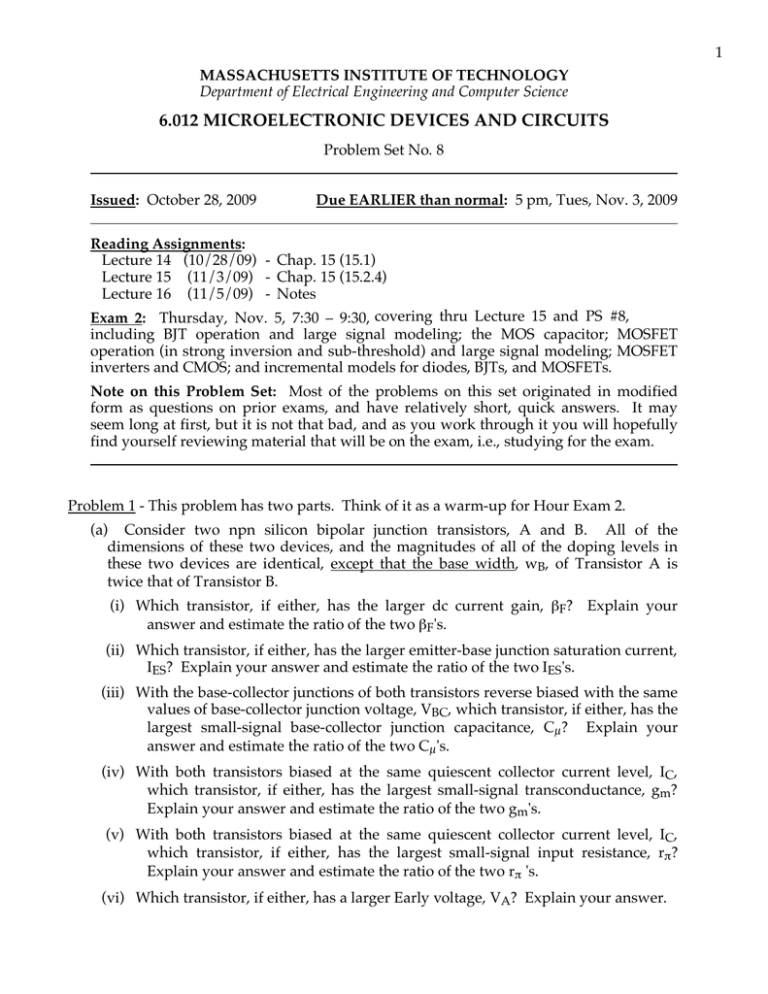
1 MASSACHUSETTS INSTITUTE OF TECHNOLOGY Department of Electrical Engineering and Computer Science 6.012 MICROELECTRONIC DEVICES AND CIRCUITS Problem Set No. 8 Issued: October 28, 2009 Due EARLIER than normal: 5 pm, Tues, Nov. 3, 2009 Reading Assignments: Lecture 14 (10/28/09) - Chap. 15 (15.1) Lecture 15 (11/3/09) - Chap. 15 (15.2.4) Lecture 16 (11/5/09) - Notes Exam 2: Thursday, Nov. 5, 7:30 – 9:30, covering thru Lecture 15 and PS #8, including BJT operation and large signal modeling; the MOS capacitor; MOSFET operation (in strong inversion and sub-threshold) and large signal modeling; MOSFET inverters and CMOS; and incremental models for diodes, BJTs, and MOSFETs. Note on this Problem Set: Most of the problems on this set originated in modified form as questions on prior exams, and have relatively short, quick answers. It may seem long at first, but it is not that bad, and as you work through it you will hopefully find yourself reviewing material that will be on the exam, i.e., studying for the exam. Problem 1 - This problem has two parts. Think of it as a warm-up for Hour Exam 2. (a) Consider two npn silicon bipolar junction transistors, A and B. All of the dimensions of these two devices, and the magnitudes of all of the doping levels in these two devices are identical, except that the base width, wB, of Transistor A is twice that of Transistor B. (i) Which transistor, if either, has the larger dc current gain, βF? Explain your answer and estimate the ratio of the two βF's. (ii) Which transistor, if either, has the larger emitter-base junction saturation current, IES? Explain your answer and estimate the ratio of the two IES's. (iii) With the base-collector junctions of both transistors reverse biased with the same values of base-collector junction voltage, VBC, which transistor, if either, has the largest small-signal base-collector junction capacitance, Cµ? Explain your answer and estimate the ratio of the two Cµ's. (iv) With both transistors biased at the same quiescent collector current level, IC, which transistor, if either, has the largest small-signal transconductance, gm? Explain your answer and estimate the ratio of the two gm's. (v) With both transistors biased at the same quiescent collector current level, IC, which transistor, if either, has the largest small-signal input resistance, rπ? Explain your answer and estimate the ratio of the two rπ 's. (vi) Which transistor, if either, has a larger Early voltage, VA? Explain your answer. 2 (b) This part involves MOSFETs. (i) Consider two MOSFETs, one an n-channel MOSFET and the other a p-channel MOSFET. They have identical dimensions, and both are biased in the saturation region at the same drain current, |ID|. Which of the devices, if either, would have the larger transconductance, gm, and why? (ii) Consider two MOSFETs, one an n-channel MOSFET and the other a p-channel MOSFET. They have identical dimensions, and both are biased in the sub threshold region at the same drain current, |ID|. Which of the devices, if either, would have the larger transconductance, gm, and why? (iii) An n-channel MOSFET operating in a circuit was mistakenly biased in the linear region. Derive expressions in terms of VGS, VDS, and K for its transconductance, gm, and output conductance, go, in this situation. Assume vBS = 0 and α = 1, and ignore the Early effect, i.e., assume λ = 0. Problem 2 - Consider the n-channel MOSFET circuit pictured to the right. The circuit is biased with VAC = VDS = 2 Volts. The MOSFET has following A parameters: D K = 2 mA/V2 VT = 1 V α=1 λ = 0.01 V-1 η = 0.2 A small signal voltage, vac(t), is added to the 2 V bias so now vAC(t) = 2 V + vac(t). + 3V ! G (a) What are the bias and small signal values of vGS, vDS, and vBS? B S C (b) Use the linear equivalent circuit (LEC) for a MOSFET to draw the full LEC for this circuit. Evaluate all of the parameter values in your LEC. (c) Reduce your LEC in Part ii) to a single element and give an expression for this element in terms of gm and go. Problem 3 - On Slide 8 in Lecture 14 the voltage gain of an NMOS inverter stage is calculated for the bias point VIN = VOUT, which is in the steep portion of the transfer characteristic. The substrate and source of the depletion mode pull-up MOSFET were shorted together, but this is not possible in many fabrication processes. Instead, the substrate of the pull-up MOSFET must be tied to ground. Redo the voltage gain calculation in this case by doing the following steps: (a) What is the small signal base-to-source voltage, vbs,pu, on the pull-up MOSFET? (b) Draw the small signal linear equivalent circuit of the pull-up MOSFET. Notice that incrementally the drain is also connected to ground so that the substrate and drain are connected incrementally. Thus the pull-up MOSFET looks like a two terminal device in this connection and its LEC is simply a resistor (i.e., rpu or gpu). Give an expression for gpu in terms of go,pu and gm,pu. (Remember gmb and gm are related.) (c) Draw the LEC for the entire inverter; be sure to indicate vin and vout. 3 (d) Derive an expression for the voltage gain, Av = vout/vin, (i) in terms of gm, gmb, and go of the two transistors, and (ii) in terms of the bias point current and K, λ, and η of the two transistors. (e) Is the gain larger or smaller than when the pull-up substrate was tied to its source, or is it no different? Explain your answer. Problem 4 - The gates on a CMOS logic chip were laid out by a designer who had not taken 6.012 and they have Wp = Wmin and Wn = 2 Wmin, instead of Wn = Wmin and Wp = 2 Wmin. What was the impact of this error on the following inverter performance metrics relative to the usual case of an inverter with Wn = Wmin and Wp = 2 Wmin? State whether each` has increased, decreased, or not changed appreciably, and explain your answers. (a) Inverter input capacitance, CL. (b) The output node charging current after the input has switched from HI to LO. (c) The output node discharge current after the input has switched from LO to HI. (d) Static power dissipation. (e) The logic HI voltage. (f)) The noise margins. MIT OpenCourseWare http://ocw.mit.edu 6.012 Microelectronic Devices and Circuits Fall 2009 For information about citing these materials or our Terms of Use, visit: http://ocw.mit.edu/terms.

