Extrinsic Semiconductors
advertisement
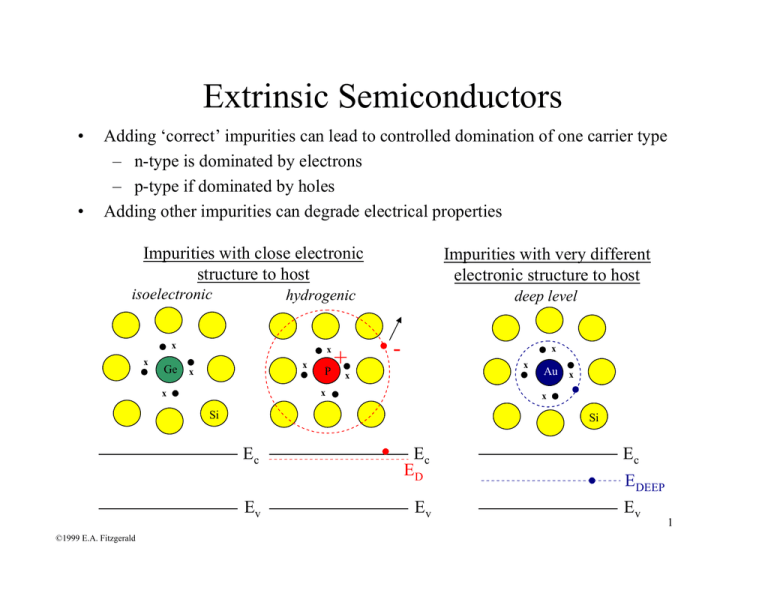
Extrinsic Semiconductors • • Adding ‘correct’ impurities can lead to controlled domination of one carrier type – n-type is dominated by electrons – p-type if dominated by holes Adding other impurities can degrade electrical properties Impurities with close electronic structure to host isoelectronic hydrogenic x x Ge Impurities with very different electronic structure to host x x x P + deep level - x x x x x x Si Si Ec Ev ©1999 E.A. Fitzgerald Au x Ec ED Ev Ec EDEEP Ev 1 Hydrogenic Model • For hydrogenic donors or acceptors, we can think of the electron or hole, respectively, as an orbiting electron around a net fixed charge • We can estimate the energy to free the carrier into the conduction band or valence band by using a modified expression for the energy of an electron in the H atom me 4 13.6 En = 2 2 2 = − 2 8ε o h n n e2 (in eV) =e me m *e 4 1 13.6 m* 1 εr En = 2 2 2 ⎯⎯⎯→ 2 2 2 2 = − 2 n m ε2 8ε oh n 8ε o h n ε r 4 2 •Thus, for the ground state n=1, we can see already that since ε is on the order of 10, the binding energy of the carrier to the center is <0.1eV •Expect that many carriers are then thermalize at room T •Experiment: •B acceptor in Si: .046 eV •P donor in Si: 0.044 eV •As donor in Si: 0.049 2 ©1999 E.A. Fitzgerald The Power of Doping • • Can make the material n-type or p-type: Hydrogenic impurities are nearly fully ionized at room temperature – ni2 for Si: ~1020cm-3 – Add 1018cm-3 donors to Si: n~Nd – n~1018cm-3, p~102 (ni2/Nd) Can change conductivity drastically – 1 part in 107 impurity in a crystal (~1022cm-3 atom density) – 1022*1/107=1015 dopant atoms per cm-3 – n~1015, p~1020/1015~105 σ/σi~(p+n)/2ni~n/2ni~105! Impurities at the ppm level drastically change the conductivity (5-6 orders of magnitude) 3 ©1999 E.A. Fitzgerald Expected Temperature Behavior of Doped Material (Example:n-type) • 3 regimes ln(n) Eg/2kb Eb/kb Intrinsic Extrinsic Freeze-out 1/T 4 ©1999 E.A. Fitzgerald Contrasting Semiconductor and Metal Conductivity ne 2τ σ= m • Semiconductors – changes in n(T) can dominate over τ – as T increases, conductivity increases • Metals – n fixed – as T increases, τ decreases, and conductivity decreases 5 ©1999 E.A. Fitzgerald General Interpretation of τ • Metals and majority carriers in semiconductors – τ is the scattering length – Phonons (lattice vibrations), impurities, dislocations, and grain boundaries can decrease τ 1 τ τi = = 1 τ phonon li 1 = vth vthσ i N i liσ i N i = 1 + 1 τ impur + 1 τ disl + 1 τ gb + ... where σ is the cross-section of the scatterer, N is the number of scatterers per volume, and l is the average distance before collisions The mechanism that will tend to dominate the scattering will be the mechanism with the shortest l (most numerous), unless there is a large difference in the cross-sections Example: Si transistor, τphonon dominates even though τimpur gets worse with scaling 6 ©1999 E.A. Fitzgerald Example: Electron Mobility in Ge 106 μ~T-3/2 if phonon dominated (T-1/2 from vth, T-1 from x-section σ -3/2 T 3 Ge (1013) At higher doping, the ionized donors are the dominate scattering mechanism µe,cm2/volt-s 105 3 (1015) 104 (1017) 3 103 10 30 100 300 T Figure by MIT OpenCourseWare. 7 ©1999 E.A. Fitzgerald Other Interpretation of τ • Minority carriers in semiconductors – can think of τ as the time to recombination: recombination time – does not affect Drude model in any way τ, l Ec Recombination event: electron disappears E Ev x Imagine p-type material, so there are many more holes than electrons holes=majority carrier electrons=minority carrier τ is referred to in this context as the minority carrier lifetime 8 ©1999 E.A. Fitzgerald Other Recombination Pathways • Deep levels in semiconductors act as carrier traps and/or enhanced recombination sites Ec Edeep Recombination through deep level E Ev x •Barrier to capture carrier is Eg/2 •Since the probability of the carrier transition is ~e-ΔE/kT, trapping a carrier with a deep state is very probable •A trapped carrier can then help attract another carrier, increasing recombination through the deep state 1 τ = 1 τ int rinsic + 1 τ deep 9 ©1999 E.A. Fitzgerald Recombination and Generation (Ec to Ev) • • Generation – intrinsic: photon-induced or thermally induced, G=#carriers/vol.-sec – extrinsic:deep levels due to traps – Go is the equilibrium generation rate Recombination – intrinsic: across band gap, R=# carriers/vol.-sec – extrinsic: deep levels due to traps – Ro is the equilibrium recombination rate, which is balanced by Go Non-equilibrium intrinsic recombination n-type material R= Δp τh ; τh = po Ro Where po is the equilibrium minority carrier concentration p-type material R= Δn τe ; τe = no Ro Where no is the equilibrium minority carrier concentration ©1999 E.A. Fitzgerald Non-equilibrium extrinsic recombination R= Δp τh τh = 1 σ h vth N t Where σh is the capture cross section for holes and Nt is the concentration of recombination centers R= Δn τe τe = 1 σ e vth N t 10
