Surface Analysis @ Warwick Surface composition
advertisement

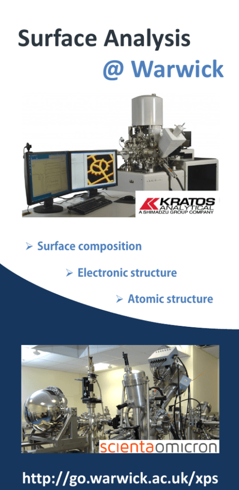
Surface Analysis @ Warwick Surface composition Electronic structure Atomic structure http://go.warwick.ac.uk/xps Complete surface analysis in high-resolution. Made possible by two world-class instruments offering monochromated XPS in conjunction with STM, LEED, ARPES and UPS. Principle of XPS XPS uses a X-ray source to stimulate the emission of electrons from the surface of a solid sample. The binding energy of these electrons are characteristic of the elements and associated chemical bonding environments in the top few atomic layers of the material. Samples can be tilted to affect the escape depth of the electrons and thus determine the thickness of overlayers on a surface. This feature is particularly relevant for adhesion and joining technology and wetting experiments, but can be used in a whole range of applications. For analysis beyond the top 2-10 nm, an inert gas ion gun can be used to sputter off the surface layers before analysis. Alternating sputtering and XPS measurements permits chemical depth profiles to be obtained. Survey scan of InN(0001) A survey scan is used to identify the peaks of interest, in this case In, N, C and O. From this, specific binding energy regions are identified for high-resolution data collection. X-ray Photoelectron Spectroscopy (XPS) The XPS capabilities on our two instruments offer a highlyaccurate determination of the composition of the surfaces of materials. Through monochromated x-ray beams and multichannel electron analysers, our instruments allow samples as small as 100 microns to be probed with a resolution of better than 0.5 eV. Both instruments are also equipped with a high-flux dual anode X-ray source for simple compositional experiments. Compositional analysis is performed by first recording a survey spectrum of the surface (left), before focusing in on the regions of interest in higher resolution (below). Our dedicated staff will be there to assist you on every step of the way, from the experiment planning to data analysis. In 3d Region in InN High-resolution XPS data from an InN surface after exposure to air, showing components from the bulk material and surface oxides. Using these data, it is possible to quantify the thickness of the oxidised layer. The various chemical environments of the In atoms are shown by the different coloured components. EXAMPLES OF RECENT WORK AT THE WARWICK PHOTOEMISSION FACILITY INCLUDE: Graphene Semiconductors Commercial plastics Biocatalysts Photovoltaics Kitchen work surfaces Nanoparticles Perovskites Carbide materials Topological insulators Transparent conducting oxides Commercial coatings & paints Complementary techniques Not just XPS…… The Omicron multiprobe instrument comprises four interconnected ultra-high vacuum (UHV) chambers. Samples are loaded in to the fast-entry chamber and pumped down to UHV conditions in under two hours. Samples can then be relocated to the preparation, XPS or ARPES chambers using the built-in transfer system. The system is also equipped with a carousel (left), in which up to twelve samples can be stored simultaneously in UHV conditions. ATOMIC STRUCTURE BY LOW ENERGY ELECTRON DIFFRACTION LEED is used to identify the periodicity of crystalline surfaces. This is a useful tool in analysing surface preparation methods and deposition experiments. IN-SITU SAMPLE PREPARATION Both of our instruments possess low energy ion guns and annealing stages for sample preparation. A thermal gas cracker and ports for deposition sources are also available (Omicron instrument). ULTRAVIOLET PHOTOELECTRON SPECTROSCOPY (UPS) In UPS, ultraviolet light originating from a helium lamp, with an energy of 21.2 eV (He I emission), illuminates the sample. The photoelectrons emitted from the surface possess energies characteristic of the valence band of the material. Fermi edge referencing with a resolution of better than 0.1 eV is possible. Angle-resolved photoemission (ARPES) ARPES is an extension of the photoemission technique where the angle of the emitted electrons is also measured. By conservation of momentum, measurement of the angle and the kinetic energy of the emitted electron allows the in-plane momentum of electrons within the solid to be determined. ARPES can probe the properties of electronic structures, such as band structure, subbands, the Fermi surface and band gap. ARPES at Warwick Left: The Scienta R4000 analyser and the ARPES vacuum chamber, also attached to which are a LEED optic and a 5-axis He-cooled manipulator. Right: Subband spectra from CdO(001) at room temperature using incident photons of 21.2 eV (He I emission). The Omicron instrument is equipped with a vacuum suitcase for transfer under UHV conditions to our scanning tunneling microscopy (STM) chamber. In STM, the surface can be imaged in atomic resolution, an extremely useful tool in surface science investigations. STM of the Si(111)-(7x7) reconstruction Dr. Marc Walker (Facility Manager) Department of Physics University of Warwick Coventry, West Midlands CV4 7AL, United Kingdom 024 761 51776 M.Walker@warwick.ac.uk http://go.warwick.ac.uk/xps

