High-performance lithium battery anodes using silicon nanowires * CANDACE K. CHAN
advertisement
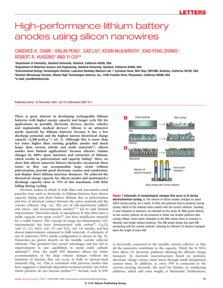
LETTERS High-performance lithium battery anodes using silicon nanowires CANDACE K. CHAN1, HAILIN PENG2, GAO LIU3, KEVIN McILWRATH4, XIAO FENG ZHANG4, ROBERT A. HUGGINS2 AND YI CUI2* 1 Department of Chemistry, Stanford University, Stanford, California 94305, USA Department of Materials Science and Engineering, Stanford University, Stanford, California 94305, USA 3 Environmental Energy Technologies Division, Lawrence Berkeley National Lab, 1 Cyclotron Road, Mail Stop 70R108B, Berkeley, California 94720, USA 4 Electron Microscope Division, Hitachi High Technologies America, Inc., 5100 Franklin Drive, Pleasanton, California 94588, USA *e-mail: yicui@stanford.edu 2 Published online: 16 December 2007; doi:10.1038/nnano.2007.411 There is great interest in developing rechargeable lithium batteries with higher energy capacity and longer cycle life for applications in portable electronic devices, electric vehicles and implantable medical devices1. Silicon is an attractive anode material for lithium batteries because it has a low discharge potential and the highest known theoretical charge capacity (4,200 mAh g21; ref. 2). Although this is more than ten times higher than existing graphite anodes and much larger than various nitride and oxide materials3,4, silicon anodes have limited applications5 because silicon’s volume changes by 400% upon insertion and extraction of lithium, which results in pulverization and capacity fading2. Here, we show that silicon nanowire battery electrodes circumvent these issues as they can accommodate large strain without pulverization, provide good electronic contact and conduction, and display short lithium insertion distances. We achieved the theoretical charge capacity for silicon anodes and maintained a discharge capacity close to 75% of this maximum, with little fading during cycling. Previous studies in which Si bulk films and micrometre-sized particles were used as electrodes in lithium batteries have shown capacity fading and short battery lifetime due to pulverization and loss of electrical contact between the active material and the current collector (Fig. 1a). The use of sub-micrometre pillars6 and micro- and nanocomposite anodes5,7–9 led to only limited improvement. Electrodes made of amorphous Si thin films have a stable capacity over many cycles5,8, but have insufficient material for a viable battery. The concept of using one-dimensional (1D) nanomaterials has been demonstrated with carbon10, Co3O4 (refs 11, 12), SnO2 (ref. 13) and TiO2 (ref. 14) anodes, and has shown improvements compared to bulk materials. A schematic of our Si nanowire (NW) anode configuration is shown in Fig. 1b. Nanowires are grown directly on the metallic current collector substrate. This geometry has several advantages and has led to improvements in rate capabilities in metal oxide cathode materials15. First, the small NW diameter allows for better accommodation of the large volume changes without the initiation of fracture that can occur in bulk or micron-sized materials (Fig. 1a). This is consistent with previous studies that have suggested a materials-dependent terminal particle size below which particles do not fracture further16,17. Second, each Si NW Initial substrate After cycling X Film X X Particles Nanowires Efficient 1D electron transport Facile strain relaxation Good contact with current collector Figure 1 Schematic of morphological changes that occur in Si during electrochemical cycling. a, The volume of silicon anodes changes by about 400% during cycling. As a result, Si films and particles tend to pulverize during cycling. Much of the material loses contact with the current collector, resulting in poor transport of electrons, as indicated by the arrow. b, NWs grown directly on the current collector do not pulverize or break into smaller particles after cycling. Rather, facile strain relaxation in the NWs allows them to increase in diameter and length without breaking. This NW anode design has each NW connecting with the current collector, allowing for efficient 1D electron transport down the length of every NW. is electrically connected to the metallic current collector so that all the nanowires contribute to the capacity. Third, the Si NWs have direct 1D electronic pathways allowing for efficient charge transport. In electrode microstructures based on particles, electronic charge carriers must move through small interparticle contact areas. In addition, as every NW is connected to the current-carrying electrode, the need for binders or conducting additives, which add extra weight, is eliminated. Furthermore, nature nanotechnology | VOL 3 | JANUARY 2008 | www.nature.com/naturenanotechnology © 2008 Nature Publishing Group 31 LETTERS 2.0 7 2 Potential versus Li/Li + (V) Discharge Current (mA) 1 0 1 –2 Charge –4 7 1.5 1.0 0.5 0.0 –6 0.0 0.5 1.0 1.5 0 2.0 1,000 2,000 3,000 4,000 5,000 Potential versus Li/Li+ (V) Capacity (mAh g–1) C/20 4,000 Capacity (mAh g–1) Potential versus Li/Li + (V) C/10 C C/2 C/5 2.0 1.5 1.0 0.5 C/10 C/20 0.0 C C/2 C/5 0 1,000 2,000 3,000 Capacity (mAh g–1) 3,000 Si NW charge Si NW discharge Si NC charge Graphite charge 2,000 1,000 0 4,000 0 2 4 6 Cycle number 8 10 Figure 2 Electrochemical data for Si NW electrodes. a, Cyclic voltammogram for Si NWs from 2.0 V to 0.01 V versus Li/Liþ at 1 mV s21 scan rate. The first seven cycles are shown. b, Voltage profiles for the first and second galvanostatic cycles of the Si NWs at the C/20 rate. The first charge achieved the theoretical capacity of 4,200 mAh g21 for Li4.4Si. c, The voltage profiles for the Si NWs cycled at different power rates. The C/20 profile is from the second cycle. d, Capacity versus cycle number for the Si NWs at the C/20 rate showing the charge (squares) and discharge capacity (circles). The charge data for Si nanocrystals (triangles) from ref. 8 and the theoretical capacity for lithiated graphite (dashed line) are shown as a comparison to show the improvement when using Si NWs. our Si NW battery electrode can be easily realized using the vapour–liquid –solid (VLS) or vapour–solid (VS) template-free growth methods18–23 to produce NWs directly onto stainless steel current collectors (see Methods). A cyclic voltammogram of the Si NW electrode is shown in Fig. 2a. The charge current associated with the formation of the Li–Si alloy began at a potential of 330 mV and became quite large below 100 mV. Upon discharge, current peaks appeared at about 370 and 620 mV. The current–potential characteristics were consistent with previous experiments on microstructured Si anodes6. The magnitude of the current peaks increased with cycling due to activation of more material to react with Li in each scan6. The small peak at 150–180 mV may have been due to reaction of the Li with the gold catalyst, which makes a negligible contribution to the charge capacity (see Supplementary Information, Figs S1 and S2). Si NWs were found to exhibit a higher capacity than other forms of Si (ref. 5). Figure 2b shows the first and second cycles at the C/20 rate (20 h per half cycle). The voltage profile observed was consistent with previous Si studies, with a long flat plateau during the first charge, during which crystalline Si reacted with Li to form amorphous LixSi. Subsequent discharge and charge cycles had different voltage profiles characteristic of amorphous Si (refs 24– 27). Significantly, the observed capacity during this first charging operation was 4,277 mAh g21, which is essentially equivalent to the theoretical capacity within experimental error. The first discharge capacity was 3,124 mAh g21, indicating a coulombic efficiency of 73%. The second charge capacity decreased by 17% to 3,541 mAh g21, although the second discharge capacity increased slightly to 3,193 mAh g21, giving a coulombic efficiency of 90%. Both charge and discharge 32 capacities remained nearly constant for subsequent cycles, with little fading up to 10 cycles (Fig. 2d), which is considerably better than previously reported results8,9. As a comparison, our charge and discharge data are shown along with the theoretical capacity (372 mAh g21) for the graphite currently used in lithium battery anodes, and the charge data reported for thin films containing 12-nm Si nanocrystals8 (NCs) in Fig. 2d. This improved capacity and cycle life in the Si NWs demonstrates the advantages of our Si NW anode design. The Si NWs also displayed high capacities at higher currents. Figure 2c shows the charge and discharge curves observed at the C/20, C/10, C/5, C/2 and 1C rates. Even at the 1C rate, the capacities remained .2,100 mAh g21, which is still five times larger than that of graphite. The cyclability of the Si NWs at the faster rates was also excellent. Using the C/5 rate, the capacity was stable at 3,500 mAh g21 for 20 cycles in another device (see Supplementary Information, Fig. S3). Despite the improved performance, the Si NW anode showed an irreversible capacity loss in the first cycle, which has been observed in other work5. Although solid electrolyte interphase (SEI) formation has been observed in Si (ref. 28), we do not believe this is the cause of our initial irreversible capacity loss, because there is no appreciable capacity in the voltage range of the SEI layer formation (0.5 –0.7 V) during the first charge (Fig. 2b)8. Although SEI formation may be occurring, the capacity involved in SEI formation would be very small compared to the high charge capacity we observed. The mechanism of the initial irreversible capacity is not yet understood and requires further investigation. The structural morphology changes during Li insertion were studied to understand the high capacity and good cyclability of our Si NW electrodes. Pristine, unreacted Si NWs were crystalline nature nanotechnology | VOL 3 | JANUARY 2008 | www.nature.com/naturenanotechnology © 2008 Nature Publishing Group LETTERS Si Ni Si Ni Number of nanowires 200 Initial 10 m V 100 0 0 100 200 Diameter (nm) 8 Current (nA) 250 nm Current (µA) 20 50 nm 300 10 0 –10 4 0 –4 –20 –0.4 0.0 0.4 Voltage (V) –0.4 0.0 0.4 Voltage (V) Figure 3 Morphology and electronic changes in Si NWs from reaction with Li. a,b, SEM image of pristine Si NWs before (a) and after (b) electrochemical cycling (same magnification). The inset in a is a cross-sectional image showing that the NWs are directly contacting the stainless steel current collector. c,d, TEM image of a pristine Si NW with a partial Ni coating before (c) and after (d) Li cycling. e, Size distribution of NWs before and after charging to 10 mV (bin width 10 nm). The average diameter of the NWs increased from 89 to 141 nm after lithiation. f, I – V curve for a single NW device (SEM image, inset) constructed from a pristine Si NW. g, I – V curve for a single NW device (SEM image, inset), constructed from a NW that had been charged and discharged once at the C/20 rate. with smooth sidewalls (Fig. 3a) and had an average diameter of 89 nm (s.d., 45 nm) (Fig. 3e). Cross-sectional scanning electron microscopy (SEM) showed that the Si NWs grew off the substrate and had good contact with the stainless steel current collector (Fig. 3a, inset). After charging with Li, the Si NWs had roughly textured sidewalls (Fig. 3b), and the average diameter increased to 141 nm (s.d., 64 nm). Despite the large volume change, the Si NWs remained intact and did not break into smaller particles. They also appeared to remain in contact with the current collector, suggesting minimal capacity fade due to electrically disconnected material during cycling. The Si NWs may also change their length during the change in volume. To evaluate this, 25-nm Ni was evaporated onto as-grown Si NWs using electron beam evaporation. Because of the shadow effect of the Si NWs, the Ni only covered part of the NW surface (Fig. 3c), as confirmed by energy dispersed X-ray spectroscopy (EDS) mapping (see Supplementary Information, Fig. S4). The Ni is inert to Li and acts as a rigid backbone on the Si NWs. After lithiation (Fig. 3d), the Si NWs changed shape and wrapped around the Ni backbone in a three-dimensionally helical manner. This appeared to be due to an expansion in the length of the NW, which caused strain because the NW was attached to the Ni and could not freely expand but rather buckled into a helical shape. Although the NW length increased after lithiation, the NWs remained continuous and without fractures, maintaining a pathway for electrons all the way from the collector to the NW tips. With both a diameter and length increase, the Si NW volume change after Li insertion appears to be about 400%, consistent with the literature5. Efficient electron transport from the current collector to the Si NWs is necessary for good battery cycling. To evaluate this, we conducted electron transport measurements on single Si NWs before and after lithiation (see Methods). The current versus voltage curve on a pristine Si NW was linear, with a 25 kV resistance (resistivity of 0.02 V-cm) (Fig. 3f ). After one cycle, the NWs became amorphous, but still exhibited a current that was linear with voltage with an 8 MV resistance (resistivity of 3 V-cm) (Fig. 3g). The good conductivity of pristine and cycled NWs ensures efficient electron transport for charge and discharge. The large volume increase in the Si NWs is driven by the dramatic atomic structure change during lithiation. To understand the structural evolution of NWs, we characterized the NW electrodes at different charging potentials. The X-ray diffraction (XRD) patterns were taken for initial pristine Si NWs, Si NWs charged to 150 mV, 100 mV, 50 mV and 10 mV, as well as after 5 cycles (Fig. 4a). XRD patterns of the as-grown Si NWs nature nanotechnology | VOL 3 | JANUARY 2008 | www.nature.com/naturenanotechnology © 2008 Nature Publishing Group 33 LETTERS α-FeSi2 (001) Au(111) From Si From SS Si (111) (111) From Au ( Li15Au4) From α-FeSi2 (220) Initial Crystal Amorphous 150 mV Intensity (a.u.) ·112Ò Crystal 100 mV Crystal 50 mV 50 nm 100 nm Amorphous 50 nm 10 mV Crystal After 5 cycles 3.3 Å 20 40 60 2θ (deg) 80 100 2 nm Amorphous Crystal Amorphous Amorphous 3.3 Å 2 nm 5 nm 40 nm Figure 4 Structural evolution of Si NWs during lithiation. a, XRD patterns of Si NWs before electrochemical cycling (initial), at different potentials during the first charge, and after five cycles. b–e, TEM data for Si NWs at different stages of the first charge. b, A single-crystalline, pristine Si NW before electrochemical cycling. The SAED spots (inset) and HRTEM lattice fringes (bottom) are from the Si 1/3(224) planes. c, NW charged to 100 mV showing a Si crystalline core and the beginning of the formation of a Lix Si amorphous shell. The HREM (bottom) shows an enlarged view of the region inside the box. d, Dark-field image of a NW charged to 50 mV showing an amorphous Lix Si wire with crystalline Si grains (bright regions) in the core. The spotty rings in the SAED (inset) are from crystalline Si. The HRTEM (bottom) shows some Si crystal grains embedded in the amorphous wire. e, A NW charged to 10 mV is completely amorphous Li4.4Si. The SAED (top) shows diffuse rings characteristic of an amorphous material. showed diffraction peaks associated with Si, a-FeSi2, Au (the Si NW catalyst) and stainless steel (SS). The a-FeSi2 forms at the interface between the SS and the Si wires during the high temperature (530 8C) NW growth process. The a-FeSi2 was not found to appreciably react with Li during electrochemical cycling, although a small amount of reaction has been reported24. After Si NWs were charged to 150 mV, the higher angle Si peaks disappeared. Only the Si(111) peak was still visible, but its intensity was greatly decreased. This is consistent with the disappearance of the initial crystalline Si and the start of the formation of amorphous LixSi. The four broad peaks that appeared in the lower angles are due to the formation of Li15Au4 (see Supplementary Information, Fig. S5). At 100 mV, the pure Au peaks disappeared, indicating that the Au had completely reacted with Li. The Si(111) peak was very weak at 100 mV, and disappeared completely at 50 mV. It appears that Si NWs remain amorphous after the first charge, consistent with the non-flat voltage charging/discharging curve in Fig. 2b. This contrasts, however, with other studies on Si electrodes25,26, which have reported the formation of crystalline, Li3.75Si at potentials less than 30 –60 mV. In situ XRD studies have determined that this crystalline phase only forms at ,50 mV for films thicker than 2 mm (ref. 27). We did not observe this to be the case in our Si NWs, most likely because of their shape and small dimensions. The local structural features of Si NWs during the first Li insertion were studied with transmission electron microscopy (TEM) and selected area electron diffraction (SAED). The asgrown Si NWs were found to be single-crystalline. Figure 4b shows an example of a typical Si NW with a k112l growth direction29. Figure 4c shows a Si NW with a k112l growth direction that was charged to 100 mV. In this case there were two phases present, as expected from the voltage profile. Both crystalline and amorphous phases were clearly seen. The distribution of the two phases was observed both across the diameter (a crystalline core and an amorphous shell) and along the length. The SAED showed the spot pattern for the crystalline phase (Si), but weak diffuse rings from the amorphous phase 34 (LixSi alloy) were also observed. Li ions must diffuse radially into the NW from the electrolyte, resulting in the core– shell phase distribution. The reason for phase distribution along the length is not yet understood. At 50 mV, the Si NW became mostly amorphous with some crystalline Si regions embedded inside the core, as seen from the dark-field image and HRTEM (Fig. 4d). The SAED showed spotty rings representative of a polycrystalline sample and diffuse rings for the amorphous phase. At 10 mV (Fig. 4e), all of the Si had changed to amorphous Li4.4Si, as indicated by the amorphous rings in the SAED. These TEM observations were consistent with the XRD results (Fig. 4a) and voltage charging curves (Fig. 2b). METHODS Si NWs were synthesized using the VLS process on stainless steel substrates using Au catalyst. The electrochemical properties were evaluated under an argon atmosphere by both cyclic voltammetry and galvanostatic cycling in a threeelectrode configuration, with the Si NWs on the stainless steel substrate as the working electrode and Li foil as both reference and counter-electrodes. No binders or conducting carbon were used. The charge capacity referred to here is the total charge inserted into the Si NW, per mass unit, during Li insertion, whereas the discharge capacity is the total charge removed during Li extraction. For electrical characterization, single Si NW devices were contacted with metal electrodes by electron-beam lithography or focused-ion beam deposition. For more detailed descriptions of NW synthesis, TEM and XRD characterization, electrochemical testing, and device fabrication, see the Supplementary Information. Received 23 July 2007; accepted 14 November 2007; published 16 December 2007. References 1. Nazri, G.-A. & Pistoia, G. Lithium Batteries: Science and Technology (Kluwer Academic/Plenum, Boston, 2004). 2. Boukamp, B. A., Lesh, G. C. & Huggins, R. A. All-solid lithium electrodes with mixed-conductor matrix. J. Electrochem. Soc. 128, 725– 729 (1981). 3. Shodai, T., Okada, S., Tobishima, S. & Yamaki, J. Study of Li3 – xMxN (M:Co, Ni or Cu) system for use as anode material in lithium rechargeable cells. Solid State Ionics 86– 88, 785 –789 (1996). 4. Poizot, P., Laruelle, S., Grugeon, S., Dupont, L. & Tarascon, J.-M. Nano-sized transition-metal oxides as negative-electrode materials for lithium-ion batteries. Nature 407, 496– 499 (2000). 5. Kasavajjula, U., Wang, C. & Appleby, A. J. Nano- and bulk-silicon-based insertion anodes for lithium-ion secondary cells. J. Power Sources 163, 1003 –1039 (2007). nature nanotechnology | VOL 3 | JANUARY 2008 | www.nature.com/naturenanotechnology © 2008 Nature Publishing Group LETTERS 6. Green, M., Fielder, E., Scrosati, B., Wachtler, M. & Moreno, J. S. Structured silicon anodes for lithium battery applications. Electrochem. Solid-State Lett. 6, A75– A79 (2003). 7. Ryu, J. H., Kim, J. W., Sung, Y.-E. & Oh, S. M. Failure modes of silicon powder negative electrode in lithium secondary batteries. Electrochem. Solid-State Lett. 7, A306 –A309 (2004). 8. Graetz, J., Ahn, C. C., Yazami, R. & Fultz, B. Highly reversible lithium storage in nanostructured silicon. Electrochem. Solid-State Lett. 6, A194 – A197 (2003). 9. Gao, B., Sinha, S., Fleming, L. & Zhou, O. Alloy formation in nanostructured silicon. Adv. Mater. 13, 816 –819 (2001). 10. Che, G., Lakshmi, B. B., Fisher, E. R. & Martin, C. R. Carbon nanotubule membranes for electrochemical energy storage and production. Nature 393, 346 –349 (1998). 11. Nam, K. T. et al. Virus-enabled synthesis and assembly of nanowires for lithium ion battery electrodes. Science 312, 885 –888 (2006). 12. Shaju, K. M., Jiao, F., Debart, A. & Bruce, P. G. Mesoporous and nanowire Co3O4 as negative electrodes for rechargeable lithium batteries. Phys. Chem. Chem. Phys. 9, 1837– 1842 (2007). 13. Park, M.-S. et al. Preparation and electrochemical properties of SnO2 nanowires for application in lithium-ion batteries. Angew. Chem. Int. Edn 46, 750– 753 (2007). 14. Armstrong, G., Armstrong, A. R., Bruce, P. G., Reale, P. & Scrosati, B. TiO2(B) nanowires as an improved anode material for lithium-ion batteries containing LiFePO4 or LiNi0.5Mn1.5O4 cathodes and a polymer electrolyte. Adv. Mater. 18, 2597 –2600 (2006). 15. Li, N., Patrissi, C. J., Che, G. & Martin, C. R. Rate capabilities of nanostructured LiMn2O4 electrodes in aqueous electrolyte. J. Electrochem. Soc. 147, 2044– 2049 (2000). 16. Yang, J., Winter, M. & Besenhard, J. O. Small particle size multiphase Li-alloy anodes for lithium-ion batteries. Solid State Ionics 90, 281– 287 (1996). 17. Huggins, R. A. & Nix, W. D. Decrepitation model for capacity loss during cycling of alloys in rechargeable electrochemical systems. Ionics 6, 57– 63 (2000). 18. Morales, A. M. & Lieber, C. M. A laser ablation method for the synthesis of crystalline semiconductor nanowires. Science 279, 208 –211 (1998). 19. Huang, M. H. et al. Catalytic growth of zinc oxide nanowires by vapor transport. Adv. Mater. 13, 113– 116 (2001). 20. Dick, K. A. et al. A new understanding of Au-assisted growth of III-V semiconductor nanowires. Adv. Funct. Mater. 15, 1603– 1610 (2005). 21. Pan, Z. W., Dai, Z. R. & Wang, Z. L. Nanobelts of semiconducting oxides. Science 291, 1947– 1949 (2001). 22. Wang, Y., Schmidt, V., Senz, S. & Gosele, U. Epitaxial growth of silicon nanowires using an aluminum catalyst. Nature Nanotech. 1, 186– 189 (2006). 23. Hannon, J. B., Kodambaka, S., Ross, F. M. & Tromp, R. M. The influence of the surface migration of gold on the growth of silicon nanowires. Nature 440, 69– 71 (2006). 24. Netz, A., Huggins, R. A. & Weppner, W. The formation and properties of amorphous silicon as negative electrode reactant in lithium systems. J. Power Sources 119 –121, 95– 100 (2003). 25. Li, J. & Dahn, J. R. An in situ X-ray diffraction study of the reaction of Li with crystalline Si. J. Electrochem. Soc. 154, A156 – A161 (2007). 26. Obrovac, M. N. & Krause, L. J. Reversible cycling of crystalline silicon powder. J. Electrochem. Soc. 154, A103 –A108 (2007). 27. Hatchard, T. D. & Dahn, J. R. In situ XRD and electrochemical study of the reaction of lithium with amorphous silicon. J. Electrochem. Soc. 151, A838 –A842 (2004). 28. Lee, Y. M., Lee, J. Y., Shim, H.-T., Lee, J. K. & Park, J.-K. SEI layer formation on amorphous Si thin electrode during precycling. J. Electrochem. Soc. 154, A515 –A519 (2007). 29. Wu, Y. et al. Controlled growth and structures of molecular-scale silicon nanowires. Nano Lett. 4, 433 –436 (2004). Acknowledgements We thank Dr Marshall for help with TEM interpretation and Professors Brongersma and Clemens for technical help. Y.C. acknowledges support from the Stanford New Faculty Startup Fund and Global Climate and Energy Projects. C.K.C. acknowledges support from a National Science Foundation Graduate Fellowship and Stanford Graduate Fellowship. Correspondence and requests for materials should be addressed to Y.C. Supplementary information accompanies this paper on www.nature.com/naturenanotechnology. Author contributions C.K.C. conceived and carried out the experiment and data analysis. H.P., G.L., K.M. and X.F.Z. assisted in experimental work. R.A.H. carried out data analysis. Y.C. conceived the experiment and carried out data analysis. C.K.C., R.A.H. and Y.C. wrote the paper. Reprints and permission information is available online at http://npg.nature.com/reprintsandpermissions/ nature nanotechnology | VOL 3 | JANUARY 2008 | www.nature.com/naturenanotechnology © 2008 Nature Publishing Group 35
