Measurement and Control of RF Power (Part II) Log Amps
advertisement
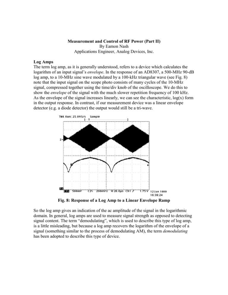
Measurement and Control of RF Power (Part II) By Eamon Nash Applications Engineer, Analog Devices, Inc. Log Amps The term log amp, as it is generally understood, refers to a device which calculates the logarithm of an input signal’s envelope. In the response of an AD8307, a 500-MHz 90-dB log amp, to a 10-MHz sine wave modulated by a 100-kHz triangular wave (see Fig. 8) note that the input signal on the scope photo consists of many cycles of the 10-MHz signal, compressed together using the time/div knob of the oscilloscope. We do this to show the envelope of the signal with the much slower repetition frequency of 100 kHz. As the envelope of the signal increases linearly, we can see the characteristic, log(x) form in the output response. In contrast, if our measurement device was a linear envelope detector (e.g. a diode detector) the output would still be a tri-wave. Fig. 8: Response of a Log Amp to a Linear Envelope Ramp So the log amp gives an indication of the ac amplitude of the signal in the logarithmic domain. In general, log amps are used to measure signal strength as opposed to detecting signal content. The term “demodulating”, which is used to describe this type of log amp, is a little misleading, but because a log amp recovers the logarithm of the envelope of a signal (something similar to the process of demodulating AM), the term demodulating has been adopted to describe this type of device. Operation of a Demodulating Log Amp The core of the simplified block diagram of a log amp (see Fig. 9) is a cascaded chain of amplifiers. These amplifiers have linear gain, usually somewhere between 10 and 20 dB. For simplicity here we have chosen a chain of 5 amplifiers, each with a gain of 20 dB, or 10X. Now, imagine a small sine wave being fed into the first amplifier in the chain. The first amplifier will gain the signal up by a factor of 10 before it is applied to the second amplifier. So as the signal passes through each subsequent stage, it is amplified by an additional 20 dB. 4V Σ 1V Det Vin 20dB 1V Det 20dB 1V Det 1V Det LOW PASS FILTER Det 20dB 20dB 20dB 1V 1V 1V Limiter Output Vlog 1V Fig. 9: Log Amp Block Diagram Now, as the signal progresses down the gain chain, it will at some stage get so big that it will begin to clip or limit at a precise level, and in this example it has been set at 1 Vpk. After the signal has gone into limiting in one of the stages (this happens at the output of the third stage in Fig. 9), the limited signal continues down the signal chain, maintaining its 1 Vpk amplitude as it goes. The signal at the output of each amplifier is also fed into a full wave rectifier (marked Det in Fig. 9.) The outputs of these rectifiers are summed together as shown, and the summer’s output is applied to a low-pass filter to remove the ripple of the rectified signal. This yields the logarithmic output (often referred to as the “video” output) which will be a steady state dc output for a steady-state ac input signal. To understand how this signal transformation yields the log of the input signal’s envelope, consider what happens if the input signal is reduced by 20 dB. As it stands in the figure, the unfiltered output of the summer is about 4 Vpk (from 3 stages that are limiting and a fourth that is just about to limit.) If we reduce the input signal by a factor of 10, one less stage will be limiting. The voltage from this stage will reduce the output of the summer to approximately 3 V. If we reduce the input signal by a further 20 dB, the summer’s output will drop to about 2 V. So the output is changing by 1 V for each 20 dB change at the input. We can describe the log amp then as having a slope of 50 mV/dB. This a key difference to a diode detector whose slope in mV/dB changes with input level. The obvious advantage of a log amp is that it has higher dynamic range and a constant slope. However, the diode detector transfer function has advantages where precision at high levels is important. Because the diode circuit has very high resolution at high input levels (i.e. more volts per dB), making small adjustments in power will be easier. Transfer Function in Terms of Slope and Intercept As in the case of the diode detector circuit, slope and intercept are the two specifications that define the transfer function of the log amp. The transfer function at 900 MHz of the AD8313, a 100-MHz to 2.5-GHz 65-dB log amp (see Fig. 10) shows that the output voltage changes by about 180 mV for a 10-dB change at the input. From this we can deduce that the slope of the transfer function is 18 mV/dB. 5 2.0 V S = +5V –100 –90 –80 4 1.6 3 1.4 2 1.2 –40 degC 1 1.0 +25 degC 0 0.8 +85 degC –1 0.6 –2 0.4 –3 0.2 0 –4 –70 –60 –50 –40 –30 –20 INPUT AMPLITUDE – dBm –10 0 10 ERROR – dB Vout - Volts 1.8 –5 Fig. 10: Slope and Intercept of a Log Amp Now, we can see that as the input signal drops down below about -65 dBm the response begins to flatten out with the device at the bottom of its range. However, if we extrapolate the linear part of the transfer function until it hits the horizontal axis, we hit a point that we call the intercept (at about -93 dBm in this case.) Note that the convention in specification of log amps is to specify this x-axis intercept, not the y-axis intercept that we use to specify diode detectors. The slope of a particular device is determined by doing a simple two-point calibration, that is, the output voltage is measured for two known input levels that are within the linear operating range. The slope is simply, Slope = (VO2-VO1)/(PI2-PI1) [1] The intercept is given by the equation, Intercept = PI1 - VO1/Slope [2] Once we know the slope and intercept of a particular device we can work out the ideal output voltage of the log amp for any input level within the linear range (about -65 dBm to 0 dBm in this case) using the simple equation, Vout = Slope(Pin-Intercept) [3] For example, if the input signal is -40 dBm the output voltage will be equal to, 18 mV/dB x (-40 dBm - (-93 dBm)) = 0.95 V It is worth noting that an increase in the intercept value decreases the output voltage. In a practical system we will be using the log amp to estimate the (unknown) input signal based upon the measured output voltage. To do this we rearrange equation [3], Pin = (Vout/Slope) + Intercept [4] Log-Conformance In the same way that we examined the linearity of a diode detector, we can plot the linearity of a log amp's response. It is somewhat confusing to talk about linearity of a log function but, more specifically, we are interested in the conformance of the device's transfer function to the log(x) mathematical function. Log-Conformance, therefore, shows the range over which the device maintains its constant slope and also shows ripple or any non-linearity over the input range. The dynamic range of the log amp is defined as the range over which the slope remains within a certain error band, usually ±1 dB or ±3 dB. In Fig. 11, for example, the ±1 dB dynamic range is approximately 95 dB (from +5 dBV to -90 dBV.) 5 4 +/- 3 dB Dynamic Range 3 2 +/- 1 dB Dynamic Range ER R OR - d B 1 0 1 0MHz -1 5 0MHz -2 -3 10 0MHz -4 -5 -1 20 -1 00 (-87d Bm) -80 -60 -40 -20 INPUT LE VEL - dBV Fig. 11: Log Conformance of a Log Amp 0 (+13dBm) 20 Temperature Stability As in the case of a diode we can also plot the log-conformance of the log amp over temperature with respect to the calculated slope and intercept at room temperature. The transfer function and log conformance of the AD8314, a 45-dB log amp, at 2.5 GHz (Fig. 12) shows that the temperature drift and log-conformance are well inside the ±1 dB error bands over a range of approximately 40 dB (-17 dBV to -57 dBV.) In precision applications the device should not be operated outside this range. Notice that for an input level of 0 dBm (-13 dBV) the log-conformance error at 25 ºC is still quite good, at about +0.7 dB. However, over temperature, especially at cold, there is a steep increase in the error to approximately -2 dB. This need to "back off" on the maximum input level to the log amp is reinforced by the fact that most wireless communications systems have their strictest emissions specifications at maximum power. 1.2 3 1. 0 2 0. 6 +85 deg C 1 +85deg C +25 deg C 0 –30 deg C 0. 4 –1 0. 2 –2 0 –70 –60 (–47dBm) –50 –40 –30 –20 INPUT AMPLIT UDE – dBV –10 (+3dBm ) Fig. 12: Temperature Stability of a Log Amp 0 –3 ERROR - dB Vup - Volts 0. 8 dBV Vs. dBm The most widely used convention in RF systems is to specify power in dBm, that is, decibels relative to 1 mW. Specification of log amp input level in terms of power is strictly a concession to popular convention; like diode detectors, they do not respond to power, but to the input voltage. The use of dBV is more correct. However, since most users specify RF signals in terms of power -- more specifically, dBm with respect to 50 Ω -- we use both dBV and dBm in specifying the performance of log amps, showing equivalent dBm levels for the special case of a 50-Ω environment. Detecting Fast RF Pulses Consider now what happens if the input signal is not continuous but pulses on and off. The response time of the log amp's output to a change at the input will be dominated by the RC time constant of the output low-pass filter (see Fig. 9, again.) With the AD8310, a 440-MHz, 95-dB log amp, responding (see Fig. 13) to a 100-MHz burst with a duration of 300 ns the 10% to 90% rise time (a popular measure of log amp response time) is about 15 ns. In practical applications, this allows us to detect and measure RF bursts as short as about 40 ns. Si gnal I nput OUTPUT 200mV PER VERTICAL DIVISION +5 V 0. 01 F 8 I NHI 52. 3 0. 01 F 0. 01 F 7 5 6 ENBL BFI N VPO S A D 8 310 I NLO COM M O FLT VO UT 1 2 3 4 GND REFERENCE INPUT 20mV PER VERTICAL DIVISION 100ns PER HORIZONTAL DIVISION Fig. 13: Log Amp Pulse Response Vo ut Figure 14. Log Amp Output Ripple Setting the bandwidth of the output low-pass filter (commonly referred to as the Video Bandwidth) very high will result in residual output ripple for input signals whose frequency is close to or below the corner frequency. The response of an AD8313 to a 10kHz input burst results in excessive output ripple (see Fig. 14) because the corner frequency of the part is internally set to around 13 MHz. This problem can, however, be easily rectified, without penalty, by adding a single-pole low-pass filter at the output. Video Bandwidth and input signal bandwidth should not be mixed up. Monolithic log amps typically have maximum input signal bandwidths that range from 50 MHz to around 2.5 GHz whereas the video bandwidths of these devices are typically in the 1 to 30 MHz range. Another interesting effect can be seen (Fig. 14, again); notice that the decay of the log amp's response seems to be quite a bit slower than that of the burst. That’s an interesting effect that results from the nature of the log transformation that is taking place. Remember, however, that at low input levels small changes in the input signal have a significant effect on the output voltage. For example, a change in the input level from 7 mV to 700 µV (or about -30 dBm to -50 dBm) has the same effect as a change in input level from 70 mV to 7 mV. Being a logarithmic amplifier, this is what you would expect. However, if we look at the input signal (i.e. the RF burst) with the naked eye, we do not see small changes in the mV range. What’s happening (in Fig. 14) is that the burst does not turn off instantly but drops to some level and then decays exponentially to zero. Now if you plot the log of a decaying exponential signal you get a straight line similar to the tail in the plot. In lab. testing of log amp pulse responses providing an input signal which has a near-ideal decay is quite challenging. A common approach is to gate the RF signal with a pulse from a generator in which pulse width can be adjusted with very high resolution3. Input Matching Log amps typically have input impedances ranging from hundreds to thousands of ohms. While reactive-matching techniques can be used to transform the typical 50 Ω source impedance to this higher level, a simple resistive shunt generally provides the best overall input match. This is especially true where there is a frequency dependency in the log amp's input impedance. In general, a shunt resistor that is slightly larger than 50 Ω is chosen, which combined in parallel with the log amp's higher input impedance gives an overall input impedance of 50 Ω. Rin (high) 52.3 Ω Fig. 15: Log Amp Input Matching A Typical RF Power Control Loop with Digital Control A typical RF power control loop which has digital control (Fig. 16) has RF signal from the PA (with a maximum power of +40 dBm) passing through a directional coupler on its way to the antenna. Directional couplers are characterized by their coupling factor which is typically in the 10- to 30-dB range, i.e. the output signal is 10 to 30 dB smaller than the primary output. Because the coupled output must deliver some power (in this case to the detector), the coupling process takes some power from the main output. This manifests itself as insertion loss, which is higher for lower coupling factors. Receive LO (PLL) Duplexer +40 dBm Power Amplifier AD6122 IF VGA 20dB Directional Coupler +20 dBm DAC 25 dB Attn. Baseband Processor -5dBm AD8314 Log Amp ADC Fig. 16: Digitally-Controlled RF Transmission System In the example shown (Fig.16) the coupled output must be attenuated by a further 25 dB before it is applied to the AD8314 log amp (recall from earlier that the AD8314 is very temperature stable for input levels below about -4 dBm.) The AD8314's output is digitized in an ADC. For an 8-bit ADC and a detector dynamic range of 40 dB, this results in a resolution of 0.16 dB/code (40dB/28.) This resolution is more than sufficient for most precision applications. Once the transmitted power is detected and digitized a DAC is used to adjust the system. In this case the power is adjusted by changing the gain of a variable gain amplifier (VGA) at IF. This is just one way in which power can be changed with other options including bias adjustment of the PA and variation of the amplitude of the baseband signal. The response time of this loop will be dominated by the digital control circuitry. In general the reaction time of the detector and the VGA will be small in comparison to the conversion rates of the ADC and DAC, and the digital processing time. A Typical Analog AGC Loop Where fast regulation of gain is required the inherent latency of a digitally-controlled AGC loop may not be acceptable. In such situations, an analog AGC loop may be a good alternative. Gain Vcontrol Vin VGA Vout Vout (dc) I Detector Vin (ac) C dV/dt = I/C R Vref (e.g. 1V) Fig. 17: An Analog Automatic Gain Control Loop Beginning at the output of the VGA in a generic version (Fig. 17) this signal is fed, usually via a directional coupler, to a detector. The output of the detector drives the input of an op amp, configured as an integrator. A reference voltage drives the non-inverting input of the op amp, and the output of the op amp integrator drives the gain-control input of the VGA. Now, let's examine how this circuit works. Assume initially that the output of the VGA is at some low level an that the reference voltage on the integrator is at 1 V. The low detector output results in a voltage drop across integrator resistor R. The resulting current through this resistor can only come from the integrator capacitor C. Current flow in this direction increases the output voltage of the integrator. This voltage, which drives the VGA, increases the gain (we are assuming that the VGA's gain control input has a positive sense, i.e. increasing voltage increases gain.) The gain will be increased, therefore increasing the amplifier's output level until the detector output equals 1 V. At that point, the current through the resistor/capacitor will decrease to zero and the integrator output will be held steady, thereby settling the loop. If capacitor charge is lost over time, the gain will begin to decrease. However, this leakage will be quickly corrected by additional integrator current from the newly-reduced detector voltage. The key usefulness of this circuit lies in its immunity to changes in the VGA gain control function. From a static perspective, at least, the relationship between gain and gain control voltage is of no consequence to the overall transfer function. Depending on the value of Vref the integrator will set the gain control voltage to whatever level is necessary to produce the desired output level. Any temperature dependency in the gain control function will be eliminated. Also, non-linearities in the gain transfer function of the VGA do not appear in the overall transfer function (Vout vs. Vref.) The only requirement is that the gain control function of the VGA be monotonic. It is crucial however that detector be temperature stable. The circuit as described so far, has been designed to produce a constant output level for varying input levels. Because this results in a constant output level it becomes clear that the detector does not require a wide dynamic range. We only require it to be temperature stable for input levels that correspond to the setpoint voltage Vref. For example, the diode detector circuits previously discussed, with poor temperature stability at low levels but reasonable stability at high levels, might be a good choice in applications where the leveled output is quite high. If, the detector we use has a higher dynamic range, we can now use this circuit to precisely set VGA output levels over a wide dynamic range. To do this the integrator reference voltage, Vref, is varied. The voltage range on Vref follows directly from the detector's transfer function. For example, if the detector delivers 0.5 V for an input level of -20 dBV, a reference voltage of 0.5 V will cause the loop to settle when the detector input is -20 dBV (the VGA output will be greater than this amount by whatever coupling factor exists between the VGA and detector.) The dynamic range for a variable Vout case is determined by the device in the loop with the least dynamic range (i.e. either the gain control range of the VGA or the linear dynamic range of the detector.) Again, note that the VGA does not need a precise gain control function. The dynamic range of the VGA's gain control in this case is defined as the range over which an increasing gain control voltage results in an increasing gain. The response time of this loop can be controlled by varying the RC time constant of the integrator. Setting this at a low level will result in fast output settling but can result in ringing in the output envelope. Setting the RC time constant high will give the loop good stability but will increase the settling time. It is interesting to note that use of the term AGC (Automatic Gain Control) to describe this circuit architecture is fundamentally incorrect. The term AGC implies that the gain is being precisely set. In practice, it is the output level that is being automatically set so the term ALC (Automatic Level Control) would be more correct. However, like the rising Sun and the direction of conventional current flow, this term is ingrained in popular terminology, so there is little point in trying to correct this inaccuracy. A Practical Analog AGC Loop In a practical AGC loop (Fig. 18) the output level of the AD603, a general purpose VGA that operates up to 90 MHz, is being controlled by the AD8314 log amp; the reference voltage is set by the AD5300, an 8-bit DAC. In addition to operation as a detector, the AD8314 incorporates the integrator required to complete the loop. We refer to this mode of operation of the detector as Controller Mode. +5 V -5 V 0.1u F V INP Vi n 2 0 -9 0 MH z 63 µV p- p -2 .8 V p-p FDBK 0.1 u F VNEG VPOS 0.1u F 0.1 u F AD603 CO M M Vo ut 20 mV p-p t o 2V p-p GPOS GNE G +1V +5 V COMM V_UP V_DN VPOS 0 .1u F CF 1 nF T HR EE- WIR E SERIAL IN TERF ACE DIN VDD SCLK AD5300 VOUT SYNC FLTR VSET RFIN +5 V ENBL AD8314 3. 0 1k Ω GND 1kΩ 1kΩ 2 kΩ Fig. 18: A Practical Analog AGC Loop The AD603 can deliver a maximum output voltage of 2 Vpk-pk. To map this maximum level into the maximum input level of the AD8314 an attenuation factor of 0.33 is required (implemented here using a simple resistor divider.) The DAC's full-scale output voltage of 5 V is likewise scaled down to correspond to the AD8314's reference voltage range (0 V to 1.25 V.) This is not absolutely necessary as we could simply use only those DAC codes which corresponds to the log amp's reference voltage range. However, scaling the DAC voltage in this manner, increases the control resolution (scaled in dB/code) by a factor of 4. As already mentioned, this circuit can be used in two distinct AGC modes. As a leveling circuit, possibly to present a constant input amplitude to an ADC, the setpoint voltage would be held constant. Alternatively, in a transmit applications where the VGA input level would be fairly constant, the setpoint voltage would be adjusted to vary the output signal amplitude by up to 45 dB. Part III of this series will deal with the response of the log amp to different signal types, and with the use of rms-to-dc converters. References 3. Design A Log Amp Pulse Detector, Microwaves & RF, January 2000. Reprints available from Analog Devices. pp 3-4 4. AD8361, Output Reference Temperature Drift Compensation, AD8361 Datasheet, pp13-14. Available at www.analog.com Biography Eamon Nash is an Applications Engineer at Analog Devices. He has worked at Analog Devices for 10 years, first as a Field Applications Engineer, based in Germany, covering mixed signal and DSP products, then as a Product-Line Applications Engineer at ADI's Advanced Linear Products Group, specializing in building-block components for instrumentation and telecommunications applications. He earned a Bachelor of Engineering degree (BEng) in Electronics from University of Limerick, Ireland. He can be contacted at 781-937-1239 (eamon.nash@analog.com) Analog Devices, Inc., 804 Woburn Street, Wilmington, MA 01887. http://www.analog.com

