a LC MOS High Speed, 8-Bit ADC with Track/Hold Function
advertisement
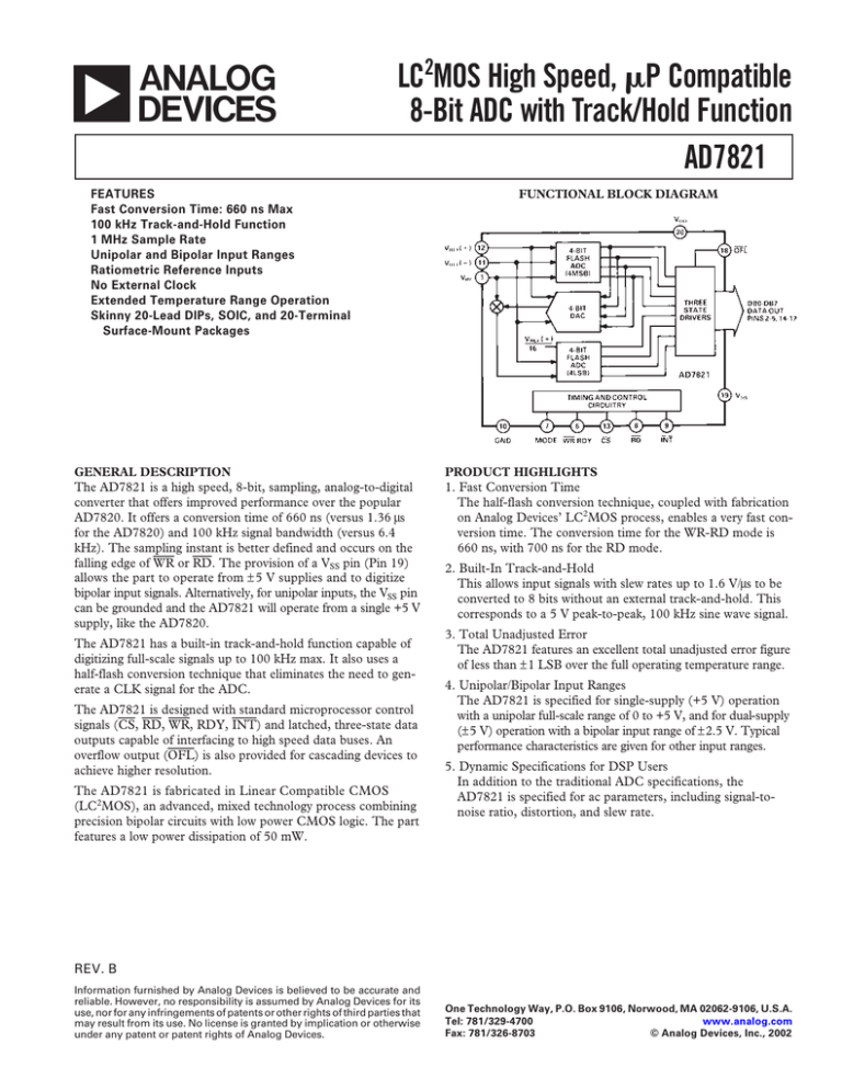
a LC2MOS High Speed, P Compatible 8-Bit ADC with Track/Hold Function AD7821 FEATURES Fast Conversion Time: 660 ns Max 100 kHz Track-and-Hold Function 1 MHz Sample Rate Unipolar and Bipolar Input Ranges Ratiometric Reference Inputs No External Clock Extended Temperature Range Operation Skinny 20-Lead DlPs, SOIC, and 20-Terminal Surface-Mount Packages FUNCTIONAL BLOCK DIAGRAM GENERAL DESCRIPTION PRODUCT HIGHLIGHTS The AD7821 is a high speed, 8-bit, sampling, analog-to-digital converter that offers improved performance over the popular AD7820. It offers a conversion time of 660 ns (versus 1.36 µs for the AD7820) and 100 kHz signal bandwidth (versus 6.4 kHz). The sampling instant is better defined and occurs on the falling edge of WR or RD. The provision of a VSS pin (Pin 19) allows the part to operate from ± 5 V supplies and to digitize bipolar input signals. Alternatively, for unipolar inputs, the VSS pin can be grounded and the AD7821 will operate from a single +5 V supply, like the AD7820. 1. Fast Conversion Time The half-flash conversion technique, coupled with fabrication on Analog Devices’ LC2MOS process, enables a very fast conversion time. The conversion time for the WR-RD mode is 660 ns, with 700 ns for the RD mode. The AD7821 has a built-in track-and-hold function capable of digitizing full-scale signals up to 100 kHz max. It also uses a half-flash conversion technique that eliminates the need to generate a CLK signal for the ADC. The AD7821 is designed with standard microprocessor control signals (CS, RD, WR, RDY, INT) and latched, three-state data outputs capable of interfacing to high speed data buses. An overflow output (OFL) is also provided for cascading devices to achieve higher resolution. The AD7821 is fabricated in Linear Compatible CMOS (LC2MOS), an advanced, mixed technology process combining precision bipolar circuits with low power CMOS logic. The part features a low power dissipation of 50 mW. 2. Built-In Track-and-Hold This allows input signals with slew rates up to 1.6 V/µs to be converted to 8 bits without an external track-and-hold. This corresponds to a 5 V peak-to-peak, 100 kHz sine wave signal. 3. Total Unadjusted Error The AD7821 features an excellent total unadjusted error figure of less than ± 1 LSB over the full operating temperature range. 4. Unipolar/Bipolar Input Ranges The AD7821 is specified for single-supply (+5 V) operation with a unipolar full-scale range of 0 to +5 V, and for dual-supply (±5 V) operation with a bipolar input range of ± 2.5 V. Typical performance characteristics are given for other input ranges. 5. Dynamic Specifications for DSP Users In addition to the traditional ADC specifications, the AD7821 is specified for ac parameters, including signal-tonoise ratio, distortion, and slew rate. REV. B Information furnished by Analog Devices is believed to be accurate and reliable. However, no responsibility is assumed by Analog Devices for its use, nor for any infringements of patents or other rights of third parties that may result from its use. No license is granted by implication or otherwise under any patent or patent rights of Analog Devices. One Technology Way, P.O. Box 9106, Norwood, MA 02062-9106, U.S.A. Tel: 781/329-4700 www.analog.com Fax: 781/326-8703 © Analog Devices, Inc., 2002 VDD = +5 V ⴞ 5%, GND = 0 V. Unipolar Input Range: VSS = GND, VREF(+) = 5 V, AD7821–SPECIFICATIONS V (–) = GND. Bipolar Input Range: V = –5 V ⴞ 5%, V (+) = 2.5 V, V (–) = –2.5 V. These test conditions apply unless otherwise stated. All specifications T to T unless otherwise noted. Specifications REF SS REF MIN REF MAX apply for RD Mode (Pin 7 = 0 V). K Version1 B, T Versions Unit 8 ±1 8 ±1 Bits LSB max 8 8 Bits 8 ±1 ±1 45 –50 –50 8 ±1 ±1 45 –50 –50 Bits LSB max LSB max dB min dB max dB max –50 –50 1.6 2.36 –50 –50 1.6 2.36 dB max dB max V/µs max V/µs typ REFERENCE INPUT Input Resistance VREF(+) Input Voltage Range VREF(–) Input Voltage Range 1.0/4.0 VREF(–)/VDD VSS/VREF(+) 1.0/4.0 VREF(–)/VDD VSS/VREF(+) kΩ min/kΩ max V min/V max V min/V max ANALOG INPUT Input Voltage Range Input Leakage Current Input Capacitance VREF(–)/VREF(+) ±3 55 VREF(–)/VREF(+) ±3 55 V min/ max µA max pF typ 2.4 0.8 1 3 –1 8 2.4 0.8 1 3 –1 8 V min V max µA max µA max µA max pF max 3.5 1.5 200 –1 8 3.5 1.5 200 –1 8 V min V max µA max µA max pF max 50 µA typ 4.0 0.4 ±3 8 4.0 0.4 ±3 8 V min V max µA max pF max ISOURCE = 360 µA ISINK = 1.6 mA Floating State Leakage Typically 5 pF 0.4 ±3 8 0.4 ±3 8 V max µA max pF max ISINK = 2.6 mA Floating State Leakage Typically 5 pF 20 100 50 ± 1/4 20 100 50 ± 1/4 mA max µA max mW typ LSB max CS = RD = 0 V CS = RD = 0 V Parameter UNIPOLAR INPUT RANGE Resolution2 Total Unadjusted Error 3 Minimum Resolution for which No Missing Codes are Guaranteed BIPOLAR INPUT RANGE Resolution2 Zero Code Error Full Scale Error Signal-to-Noise Ratio (SNR) 3 Total Harmonic Distortion (THD) 3 Peak Harmonic or Spurious Noise 3 Intermodulation Distortion (IMD) 3 Slew Rate, Tracking 3 LOGIC INPUTS CS, WR, RD VINH VINL IINH (CS, RD) IINH (WR) IINL Input Capacitance 4 MODE VINH VINL IINH IINL Input Capacitance 4 LOGIC OUTPUTS DB0–DB7, OFL, INT VOH VOL IOUT (DB0–DB7) Output Capacitance 4 (DB0–DB7) RDY VOL IOUT Output Capacitance 4 POWER SUPPLY IDD5 ISS Power Dissipation Power Supply Sensitivity Comments VIN = 99.85 kHz Full-Scale Sine Wave with f SAMPLING = 500 kHz VIN = 99.85 kHz Full-Scale Sine Wave with f SAMPLING = 500 kHz VIN = 99.85 kHz Full-Scale Sine Wave with f SAMPLING = 500 kHz fa (84.72 kHz) and fb (94.97 kHz) Full-Scale Sine Waves with fSAMPLING = 500 kHz Second Order Terms Third Order Terms –5 V ≤ VIN ≤ +5 V Typically 5 pF Typically 5 pF ± 1/16 LSB typ, V DD = 4.75 V to 5.25 V, (VREF(+) = 4.75 V max for Unipolar Mode) NOTES 1 Temperature Ranges are as follows: K Version = –40°C to +85°C; B Version = –40°C to +85°C; T Version = –55°C to +125°C. 2 1 LSB = 19.53 mV for both the unipolar (0 V to +5 V) and bipolar (–2.5 V to +2.5 V) input ranges. 3 See Terminology. 4 Sample tested at +25°C to ensure compliance. 5 See Typical Performance Characteristics. Specifications subject to change without notice. –2– REV. B AD7821 TIMING CHARACTERISTICS1 (VDD = +5 V ⴞ 5%, VSS = 0 V or –5 V ⴞ 5%; Unipolar or Bipolar Input Range) Parameter Limit at +25ⴗC (All Versions) Limit at TMIN, TMAX (K, B Versions) Limit at TMIN, TMAX (T Version) Unit Conditions/Comments tCSS tCSH tRDY2 0 0 70 0 0 85 0 0 100 ns min ns min ns max tCRD tACC03 700 875 975 ns max tCRD + 25 tCRD + 50 50 80 15 60 350 250 10 250 160 tCRD + 30 tCRD + 65 – 85 15 70 425 325 10 350 205 tCRD + 35 tCRD + 75 – 90 15 80 500 400 10 450 240 ns max ns max ns typ ns max ns min ns max ns min ns min µs max ns min ns min CS to RD/WR Setup Time CS to RD/WR Hold Time CS to RDY Delay. Pull-Up Resistor 5 kΩ Conversion Time (RD Mode) Data Access Time (RD Mode) CL = 20 pF CL = 100 pF RD to INT Delay (RD Mode) 160 185 150 380 500 65 205 235 185 – 610 75 240 275 220 – 700 85 ns max ns max ns max ns typ ns max ns min 65 90 80 75 110 100 85 130 120 ns max ns max ns max 30 45 35 60 40 70 ns max ns max tINTH2 tDH4 tP tWR tRD tREAD1 tACC13 tRI tINTL2 tREAD2 tACC23 tIHWR2 tID3 Data Hold Time Delay Time Between Conversions Write Pulsewidth Delay Time between WR and RD Pulses RD Pulsewidth (WR-RD Mode, see Figure 12b) Determined by tACC1 Data Access Time (WR-RD Mode, see Figure 12b) CL = 20 pF CL = 100 pF RD to INT Delay WR to INT Delay RD Pulsewidth (WR-RD Mode, see Figure 12a) Determined by tACC2 Data Access Time (WR-RD Mode, see Figure 12a) CL = 20 pF CL = 100 pF WR to INT Delay (Stand-Alone Operation) Data Access Time after INT (Stand-Alone Operation) CL = 20 pF CL = 100 pF NOTES 1 Sample tested at +25°C to ensure compliance. All input control signals are specified with tRISE = tFALL = 5 ns (10% to 90% of +5 V) and timed from a voltage level of 1.6 V. 2 CL = 50 pF. 3 Measured with load circuits of Figure 1 and defined as the time required for an output to cross 0.8 V or 2.4 V. 4 Defined as the time required for the data lines to change 0.5 V when loaded with the circuits of Figure 2. Specifications subject to change without notice. ORDERING GUIDE Test Circuits a. High Z to VOH b. High Z to VOL Figure 1. Load Circuits for Data Access Time Test Model1 Temperature Range Total Unadjusted Package Error (LSB) Option2 AD7821KN AD7821KP AD7821KR AD7821BQ AD7821TQ AD7821TE –40°C to +85°C –40°C to +85°C –40°C to +85°C –40°C to +85°C –55°C to +125°C –55°C to +125°C ± 1 max ± 1 max ± 1 max ± 1 max ± 1 max ± 1 max N-20 P-20A RW-20 Q-20 Q-20 E-20A NOTES 1 To order MIL-STD-883, Class B processed parts, add /883B to part number. Contact local sales office for military data sheet. 2 E = Leadless Ceramic Chip Carrier; N = Plastic DIP; P = Plastic Leaded Chip Carrier; Q = Cerdip; R = SOIC. a. VOH to High Z b. VOL to High Z Figure 2. Load Circuits for Data Hold Time Test REV. B –3– AD7821 Industrial (B Version) . . . . . . . . . . . . . . . . –40°C to +85°C Extended (T Version) . . . . . . . . . . . . . . . –55°C to +125°C Storage Temperature Range . . . . . . . . . . . . –65°C to +150°C Lead Temperature (Soldering, 10 sec) . . . . . . . . . . . . +300°C Power Dissipation (Any Package) to +75°C . . . . . . . 450 mW Derates above +75°C by . . . . . . . . . . . . . . . . . . . . . 6 mW/°C ABSOLUTE MAXIMUM RATINGS* VDD to GND . . . . . . . . . . . . . . . . . . . . . . . . . . . –0.3 V, + 7 V VSS to GND . . . . . . . . . . . . . . . . . . . . . . . . . . . . +0.3 V, + 7 V Digital Input Voltage to GND (Pins 6–8, 13) . . . . . . . . . . . . . . . . . . . –0.3 V, VDD + 0.3 V Digital Output Voltage to GND (Pins 2–5, 9, 14–18) . . . . . . . . . . . . . . . –0.3 V, VDD + 0.3 V VREF(+) to GND . . . . . . . . . . . . . . . VSS – 0.3 V, VDD + 0.3 V VREF(–) to GND . . . . . . . . . . . . . . . VSS – 0.3 V, VDD + 0.3 V VIN to GND . . . . . . . . . . . . . . . . . . . VSS – 0.3 V, VDD + 0.3 V Operating Temperature Range Commercial (K Version) . . . . . . . . . . . . . . –40°C to +85°C *Stresses above those listed under “Absolute Maximum Ratings” may cause permanent damage to the device. This is a stress rating only and functional operation of the device at these or any other conditions above those indicated in the operational sections of this specification is not implied. Exposure to absolute maximum rating conditions for extended periods may affect device reliability. CAUTION ESD (electrostatic discharge) sensitive device. Electrostatic charges as high as 4000 V readily accumulate on the human body and test equipment and can discharge without detection. Although the AD7821 features proprietary ESD protection circuitry, permanent damage may occur on devices subjected to high energy electrostatic discharges. Therefore, proper ESD precautions are recommended to avoid performance degradation or loss of functionality. DIP AND SOIC PIN CONFIGURATIONS LCCC WARNING! ESD SENSITIVE DEVICE PLCC PIN FUNCTION DESCRIPTIONS Pin Mnemonic Description 1 2 3–5 6 7 VIN DB0 DB1–DB3 WR/RDY MODE 8 9 RD INT 10 11 GND VREF(–) 12 VREF(+) 13 14–16 17 18 CS DB4–DB6 DB7 OFL 19 VSS 20 VDD Analog Input: Range V REF(–) ≤ VIN ≤ VREF(+) Three-State Data Output (LSB) Three-State Data Outputs WRITE control input/READY status output. See Digital Interface section. Mode Selection Input. It determines whether the device operates in the WR-RD or RD mode. This input is internally pulled low through a 50 µA current source. See Digital Interface section. READ Input. RD must be low to access data from the part. See Digital Interface section. INTERRUPT Output. INT going low indicates that the conversion is complete. INT returns high on the rising edge of CS or RD. See Digital Interface section. Ground Lower limit of reference span. Range: VSS ≤ VREF(–) ≤ VREF(+). Upper limit of reference span. Range: VREF(–) < VREF(+) ≤ VDD. Chip Select Input. The device is selected when this input is low. Three-State Data Outputs Three-State Data Output (MSB) Overflow Output. If the analog input is higher than (V REF(+) – 1/2 LSB), OFL will be low at the end of conversion. It is a non-three-state output which can be used to cascade two or more devices to increase resolution. Negative Supply Voltage VSS = 0 V; Unipolar Operation VSS = –5 V; Bipolar Operation Positive Supply Voltage, +5 V –4– REV. B AD7821 TERMINOLOGY LEAST SIGNIFICANT BIT (LSB) INTERMODULATION DISTORTION An ADC with 8-bit resolution can resolve one part in 28 (1/256 of full scale). For the AD7821 operating in either the unipolar or bipolar input range with 5 V full scale, one LSB is 19.53 mV. TOTAL UNADJUSTED ERROR This is a comprehensive specification which includes relative accuracy, offset error, and full-scale error. SLEW RATE Slew rate is the maximum allowable rate of change of input signal such that the digital sample values are not in error. TOTAL HARMONIC DISTORTION (THD) Total harmonic distortion is the ratio of the square root of the sum of the squares of the rms value of the harmonics to the rms value of the fundamental. For the AD7821, total harmonic distortion is defined as ( ) 2 2 2 2 2 V2 + V3 + V4 + V5 + V6 20 log dB V1 where V1 is the rms amplitude of the fundamental and V2, V3, V4, V5, and V6 are the rms amplitudes of the individual harmonics. REV. B With inputs consisting of sine waves at two frequencies, fa and fb, any active device with nonlinearities will create distortion products, of order (m+n), at sum and difference frequencies of mfa+nfb, where m, n = 0, 1, 2, 3…. Intermodulation terms are those for which m or n is not equal to zero. For example, the second order terms include (fa + fb) and (fa – fb), and the third order terms include (2fa + fb), (2fa – fb), (fa + 2fb) and (fa – 2fb). For the AD7821 intermodulation distortion is calculated separately for both the second and third order terms. SIGNAL-TO-NOISE RATIO (SNR) Signal-to-noise ratio is measured signal-to-noise at the output of the ADC. The signal is the rms magnitude of the fundamental. Noise is the rms sum of all nonfundamental signals (excluding dc) up to half the sampling frequency. SNR is dependent on the number of quantization levels used in the digitization process. The theoretical SNR for a sine wave input is given by: SNR = (6.02N + 1.76) dB where N is the number of bits in the ADC. Thus, for an ideal 8-bit ADC, SNR = 50 dB. PEAK HARMONIC OR SPURIOUS NOISE Peak harmonic or spurious noise is the rms value of the largest nonfundamental frequency (excluding dc) up to half the sampling frequency to the rms value of the fundamental. –5– AD7821—Typical Performance Characteristics TPC 1. Conversion Time (RD Mode) vs.Temperature TPC 4. Accuracy vs. tRD TPC 7. Effective Number of Bits vs. Input Signal (±2.5 V) Frequency TPC 2. Power Supply Current vs. Temperature (Not Including Reference Ladder) TPC 3. Accuracy vs. tWR TPC 5. Accuracy vs. tP TPC 6. Accuracy vs. VREF [VREF = VREF(+) – VREF(–)] TPC 8. tINTL, Internal Time Delay vs. Temperature –6– TPC 9. Output Current vs. Temperature REV. B AD7821 CIRCUIT INFORMATION BASIC DESCRIPTION The AD7821 uses a half flash conversion technique (see Functional Block Diagram), whereby two 4-bit flash ADCs are used to achieve an 8-bit result. Each 4-bit flash ADC contains 15 comparators, which compare an unknown input voltage to the reference ladder, to achieve a 4-bit result. The MS (most significant) flash ADC converts an unknown analog input voltage (VIN) to provide the 4 MS data bits. An internal DAC, driven by the 4 MS data bits, then recreates an analog approximation of the input voltage. The DAC output voltage is subtracted from the analog input, and the difference is converted by the LS (least significant) ADC to provide the 4 LS data bits. The MS flash ADC also has one additional comparator to detect over-range on the analog input. OPERATING SEQUENCE As a result, the analog input (VIN) of the device can easily be set up to provide both unipolar and bipolar operation. The data output code for unipolar and bipolar operation is Natural Binary and Offset Binary, respectively. The span of the analog input voltage can easily be varied. By reducing the reference span, VREF(+) – VREF(–), to less than 5 V, the sensitivity of the converter can be increased (i.e., if VREF = 2 V then 1 LSB = 7.8 mV). The reference flexibility also allows the input span for unipolar operation to be offset from zero (VREF(–) > GND). Additionally, the input/reference arrangement facilitates ratiometric operation. Figures 4 and 5 show some configurations that are possible. For minimum noise, a 47 µF capacitor in parallel with a 0.1 µF capacitor should be connected between the reference inputs and GND. The AD7821 has two operating modes. The RD mode allows a conversion to be started and data to be read with a single, extended, READ operation (i.e., CS and RD are taken low). The conversion process is timed out by internal one-shots. The WR-RD mode uses WR to start a conversion and RD to read the data and allows the conversion timing to be externally controlled. The operating sequence for the WR-RD mode is shown in Figure 3. Figure 4. Power Supply as Reference; Unipolar Operation (0 to + 5 V) Figure 3. Operating Sequence (WR-RD Mode) A conversion is initiated and the analog input signal (VIN) sampled on the falling edge of WR (falling edge of RD, RD mode). A setup time (tP, delay time between conversions) of 350 ns is required prior to this falling edge. See the Digital Interface section for more details. When WR is low, the internal MS (most significant) ADC compares the sampled analog input with the reference ladder to provide the 4 MS data bits. A minimum of 250 ns is required for this comparison. On the rising edge of WR, the MS data result is latched internally and the LS (least significant) conversion begins, to yield the 4 LS data bits. INT goes low typically 380 ns after the rising edge of WR. This indicates the LS conversion is complete and that both the LS and MS data results are latched into the output buffer. RD going low then enables the output data. If a faster conversion time is required, the RD line can be brought low 250 ns after WR goes high. This latches both the LS and MS data bits and outputs the conversion result on DB0–DB7. Figure 5. External Reference; Bipolar Operation (–2.5 V to +2.5 V) INPUT CURRENT REFERENCE AND INPUT The VREF(–) and VREF(+) reference inputs on the AD7821 are fully differential and define the zero and full-scale input range of the ADC. The transfer characteristic of the part is defined by the integer value of the following expression: V IN − V REF (−) Data (LSBs ) = 256 + 0.5 V REF (+) − V REF (−) REV. B The analog input of the AD7821 behaves somewhat differently than conventional ADCs. This is due to the ADC’s sampled data comparators, which take varying amounts of input current depending on the cycle of the converter. The equivalent input circuit of the AD7821 is shown in Figure 6. When a conversion ends (e.g., falling edge of INT, WR-RD mode, tRD > tINTL) all the input switches are closed and VIN is connected to the comparators of the internal LS and MS ADCs. Therefore, VIN is simultaneously connected to 31 input capacitors of 1 pF each. –7– AD7821 INHERENT TRACK-AND-HOLD A major benefit of the AD7821’s input structure is its ability to measure a variety of high speed signals without the help of an external track-and-hold. Any ADC which does not have a built-in track-and-hold, regardless of its speed, requires the analog input to remain stable to at least 1/2 LSB for the duration of the conversion to maintain full accuracy. This requires the use of a track-and-hold whenever the input is a high-speed signal. The AD7821’s sampled-data comparators, by nature of their input switching, inherently accomplish this track-and-hold function. Although the conversion time for the AD7821 is 660 ns (WR-RD mode, tWR + tRD + tACC1), the time for which VIN must be stable to 1/2 LSB is much smaller. The AD7821 tracks VIN between conversions only, and its value on the falling edge of WR or RD in the WR-RD or RD modes, respectively, is the measured value. Figure 6. AD7821 Equivalent Input Circuit SINUSOIDAL INPUTS The input capacitors must charge to the input voltage through the on resistance of the analog switches (about 2 kΩ to 5 kΩ). In addition, about 12 pF of input stray capacitance must be charged. The bandwidth of the built-in track-and-hold is 100 kHz max (150 kHz typ, 5 V p-p). This is limited by the analog bandwidth of the comparators and timing skew between the comparator switches. This means that the analog input frequency can be up to 100 kHz without the aid of an external track-and-hold. The Nyquist criterion requires that the sampling rate be at least twice the input frequency (i.e., ≥2 ⫻ 100 kHz). This requires an ideal antialiasing filter with an infinite roll-off. To ease the problem of antialiasing filter design, the sampling rate is usually set much greater than the Nyquist criterion. The maximum sampling rate (fMAX) for the AD7821 in the WR-RD mode, (tRD < tINTL) can be calculated as follows: The analog input can be modeled as an equivalent RC network as shown in Figure 7. As RS (source impedance) increases, the input capacitance takes longer to charge. The comparators track the analog input between conversions. A minimum delay time (tP) of 350 ns is required between conversions to allow for voltage source settling and comparator tracking time. This allows input time constants of 50 ns without settling time problems. Typical total input capacitance values of 55 pF allow RS to be 0.9 kΩ without lengthening tP to give VIN more time to settle. f MAX = 1 tWR + t RD + t RI + t P f MAX = (0.25 × 10 ) + (0.25 × 10 ) + (0.15 × 10 ) + (0.35 × 10 ) 1 −6 −6 −6 −6 tWR = Write Pulsewidth tRD = Delay Time between WR and RD Pulses tRI = RD to INT Delay tP = Delay Time between Conversions Figure 7. RC Network Model This permits a maximum sampling rate for the AD7821 of 1 MHz, which is much greater than the Nyquist criterion for sampling a 100 kHz analog input signal. INPUT TRANSIENTS Transients on the analog input signal caused by charging current flowing into VIN will not normally degrade the ADC’s performance. In effect, the AD7821 does not “look” at the input when these transients occur. The comparators’ inputs track VIN and are not sampled until the falling edge of WR (WR-RD Mode) or RD (RD Mode), so at least 350 ns (tP) is provided to charge the ADC’s input capacitance. It is, therefore, not necessary to filter out these transients with an external capacitor at the VIN terminal. DIGITAL SIGNAL PROCESSING APPLICATIONS In Digital Signal Processing (DSP) application areas such as voice recognition, echo cancellation, and adaptive filtering, the dynamic characteristics (Signal-to-Noise Ratio, Harmonic Distortion, Intermodulation Distortion) of an ADC are critical. Since the AD7821 is a very fast ADC with a built-in track-and-hold function, it is specified dynamically as well as with standard dc specifications (Total Unadjusted Error, and so on). –8– REV. B AD7821 SIGNAL-TO-NOISE RATIO AND DISTORTION The dynamic performance of the AD7821 is evaluated by applying a very low distortion sine wave signal to the analog input (VIN) which is then sampled at a 512 kHz sampling rate. A Fast Fourier Transform (FFT) plot is then generated from which Signal-to-Noise Ratio (SNR) and harmonic distortion data are obtained. Figure 8 shows a 2048 point FFT plot of the AD7821 with an input signal of 100.25 kHz. The SNR is 49.1 dB. It should be noted that the harmonics are taken into account when calculating the SNR. The theoretical relationship between SNR and resolution (N) is expressed by the following equation: SNR = (6.02N + 1.76) dB (1) possible to plot a histogram showing the frequency of occurrence of each of the 256 ADC codes. A perfect ADC produces a probability density function described by the equation: P(V ) = 1 π( A2 − V 2 )1/2 where A is the peak amplitude of the sine wave and P(V) is the probability of occurrence at a voltage V. If a particular step is wider than the ideal 1 LSB width, then the code associated with that step will accumulate more counts than for the code for an ideal step. Likewise, a step narrower than the ideal width will have fewer counts. Missing codes are easily seen because a missing code means zero counts for a particular code. The absence of large spikes in the plot indicates small differential nonlinearity. Figure 10 shows a histogram plot for the AD7821, which corresponds very well with the ideal shape. The plot indicates very small differential nonlinearity and no missing codes for an input frequency of 100.25 kHz. Figure 8. FFT Plot EFFECTIVE NUMBER OF BITS By working backwards from Equation (1) it is possible to get a measure of ADC performance expressed in effective number of bits (N). A plot of the effective number of bits versus input frequency is given in the Typical Performance Characteristics section. The effective number of bits typically falls between 7.7 and 7.9, corresponding to SNR figures of 48.1 dB and 49.7 dB. Figure 10. Histogram Plot INTERMODULATION DISTORTION For intermodulation distortion (IMD), an FFT plot consisting of very low distortion sine waves at two frequencies is generated by sampling an analog input applied to the ADC. Figure 9 shows a 2048 point plot for IMD. In digital signal processing applications, where the AD7821 is used to sample ac signals, it is essential that the signal sampling occurs at exactly equal intervals. This minimizes errors due to sampling uncertainty or jitter. A precise timer or clock source, to start the ADC conversion process, is the best method of generating equidistant sampling intervals. The two modes of operation given in the data sheet are suitable for DSP applications because the sampling instant of the AD7821 is well defined. VIN is sampled on the falling edge of WR or RD in the WR-RD or RD modes, respectively. DIGITAL INTERFACE The AD7821 has two basic interface modes which are determined by the status of the MODE pin. When this pin is low, the converter is in the RD mode, with this pin high, the AD7821 is set up for the WR-RD mode. Figure 9. FFT Plot for IMD HISTOGRAM PLOT When a sine wave of specified frequency is applied to the VIN input of the AD7821 and several thousand samples are taken, it is REV. B The RD mode is designed for microprocessors that can be driven into a WAIT state. A READ operation (i.e., CS and RD are taken low) starts a conversion and data is read when the conversion is complete. The WR-RD mode does not require microprocessor WAIT states. A WRITE operation (i.e., CS and WR are taken low) initiates a conversion, and a READ operation reads the result when the conversion is complete. –9– AD7821 RD Mode (MODE = 0) The timing diagram for the RD mode is shown in Figure 11. This mode is intended for use with microprocessors that have a WAIT state facility, whereby a READ instruction cycle can be extended to accommodate slow memory devices. A conversion is started by taking CS and RD low (READ operation). Both CS and RD are then kept low until output data appears. Figure 12a. WR-RD Mode (tRD > tINTL) The alternative option can be used to shorten the conversion time. This is a method for bypassing the internal time-out circuit. The INT line is ignored and RD can be brought low 250 ns after the rising edge of WR. In this case RD going low transfers the data result into the output latch and activates the data output (DB0–DB7). INT is driven low on the falling edge of RD and is reset on the rising edge of RD or CS. The timing for this interface is shown in Figure 12b. Figure 11. RD Mode In this mode, Pin 6 of the AD7821 is configured as a status output, RDY. This RDY output can be used to drive the processor READY or WAIT input. It is an open-drain output (no internal-pull-up device) which goes low after the falling edge of CS and goes high impedance at the end of conversion. An INT line is also provided which goes low when a conversion is complete. INT returns high on the rising edge of CS or RD. WR-RD Mode (MODE = 1) In the WR-RD mode, Pin 6 is configured as a WRITE (WR) input for the AD7821. With CS low, conversion is initiated on the falling edge of WR. Two options exist for reading data from the converter. In the first of these options the processor waits for the INT status line to go low before reading the data (see Figure 12a). INT typically goes low within 380 ns after the rising edge of WR. It indicates that conversion is complete and that the data result is in the output latch. With CS low, the data outputs (DB0–DB7) are activated when RD goes low. INT is reset by the rising edge of RD or CS. Figure 12b. WR-RD Mode (tRD < tINTL) The AD7821 can also be used in standalone operation in the WR-RD mode. CS and RD are tied low, and a conversion is initiated by bringing WR low. Output data is valid 530 ns (tINTL + tID) after the rising edge of WR. The timing diagram for this mode is shown in Figure 13. Figure 13. WR-RD Mode Stand-Alone Operation, CS = RD = 0 –10– REV. B AD7821 MICROPROCESSOR INTERFACING AD7821 – TMS32010 INTERFACE The AD7821 is designed for easy interfacing to microprocessors as a memory mapped peripheral or an I/O device. This reduces to a minimum the amount of external logic required for interfacing. A typical interface to the TMS32010 is shown in Figure 16. The AD7821 is mapped at a port address and the interface is designed for the maximum TMS32010 clock frequency of 20 MHz. In this case, the AD7821 is configured in the WR-RD interface mode. This means that a write instruction starts a conversion and a read instruction reads the result when the conversion is completed. A precise timer or clock source is used to start a conversion in applications requiring equidistant sampling intervals. The scheme used, whereby the AD7821 generates an interrupt to the TMS32010, is limited in that it does not allow the AD7821 to be sampled at its maximum rate. This is because the time between samples has to be long enough to allow the TMS32010 to service its interrupt and read data from the AD7821. Constant interruption of the TMS32010 by the AD7821, every time the ADC completes a conversion, is not a very efficient use of the processor time. To overcome these problems, some buffer memory or FIFO could be placed between the AD7821 and the TMS32010. The INT line of the AD7821 could be used to trigger a pulse which drives its CS and RD lines and places the AD7821 data into a FIFO or buffer memory. The microprocessor can then read a batch of data from the FIFO or buffer memory at some convenient time. Reading data from the AD7821, after an INT has been received, consists of a <IN A, PA> instruction (PA is the decoded ADC address). AD7821 – 68008 INTERFACE Figure 14 shows an AD7821 interface to the 68008 microprocessor. The ADC is configured for the RD interface mode. This means that one read instruction starts a conversion and reads the result when the conversion is completed. The read cycle is stretched out over the entire conversion period by taking the INT line back to the DTACK input of the 68008. Starting a conversion and reading the relevant data consists of a <MOVE B Dn, addr> instruction, where addr is the decoded ADC address and Dn is the data register into which the result is placed. Figure 14. AD7821 to 68008 Interface AD7821 – 8088 INTERFACE A typical interface to the 8088 is shown in Figure 15. The AD7821 is configured for the RD interface mode. One read instruction starts a conversion and reads the result. The read cycle is stretched out over the entire conversion period by taking the RDY line back to the READY input of the 8088. Starting a conversion and reading the result consists of a <MOV AX, (addr)> instruction, where addr is the decoded ADC address and AX is the 8088 data register into which the conversion result is placed. Figure 16. AD7821 to TMS32010 Interface AD7821 – 8051 INTERFACE Figure 17 shows the AD7821 interface to the 8051 microcomputer. The AD7821 is configured in the WR-RD interface mode and is connected to the 8051 ports. The processor starts conversion and then polls INT, until it goes low, before reading the conversion result. Data is read from the AD7821 by using the <MOV A, 90H> instruction (90H is the address for Port 1). Figure 15. AD7821 to 8088 Interface Figure 17. AD7821 to 8051 Interface REV. B –11– AD7821 APPLYING THE AD7821 BIPOLAR OPERATION The AD7821 is specified for a unipolar input range of 0 V to +5 V and a bipolar input range of –2.5 V to +2.5 V. The VREF(–) and VREF(+) voltages required for these input ranges are outlined below. See the Typical Performance Characteristics section for operation with unspecified input voltage ranges. Figure 18 gives the configuration and reference voltages required for –2.5 V to +2.5 V operation. The nominal transfer characteristic for this input range is shown in Figure 20. The output code is Offset Binary with 1 LSB = ([+2.5 – (–2.5)]/256) V = 19.5 mV. UNIPOLAR OPERATION Figure 18 gives the configuration and reference voltages required for 0 V to +5 V operation. The nominal transfer characteristic for this input range is shown in Figure 19. The output code is Natural Binary with 1 LSB = (5/256) V = 19.5 mV. Figure 20. Nominal Transfer Characteristic for Bipolar (–2.5 V to +2.5 V) Operation 16-CHANNEL TELECOM A/D CONVERTER Figure 18. Unipolar/Bipolar Operation The fast sampling rate (1 MHz) and bipolar operation of the AD7821 makes it useful in telecom applications for sampling a number of input channels using a multiplexer. Figure 21 shows a circuit for such an application. The maximum signal frequency required for acceptable quality in telecom applications is 3 kHz. The circuit given in Figure 21 permits each of the 16-input channels to be sampled at a rate of 16 kHz maximum. The sampling rate takes into account such multiplexer parameters as tON, settling time, and so on. The circuit also eases the problem of the antialiasing filter design by sampling at a rate much greater than that required by the Nyquist criterion. Figure 19. Nominal Transfer Characteristic for Unipolar (0 V to +5 V) Operation –12– REV. B AD7821 Figure 21. 16-Channel Telecom ADC System SIMULTANEOUS SAMPLING ADC S The AD7821’s inherent track-and-hold and well defined sampling instant makes it useful in such applications as sonar, where a number of input channels are required to be sampled simultaneously. Figure 22 shows a circuit for such an application. Figure 22. Simultaneous Sampling ADCs The actual sampling instant at which VIN is measured occurs approximately 50 ns after the falling edge of WR or RD in the WR-RD or RD modes, respectively, due to internal logic delays. However, the internal logic delay and, therefore, the sampling instant can vary from device to device, but is typically within ±5 ns. This means that a maximum common input sine wave of ± 2.5 V at 32 kHz, applied to any number of AD7821s in the circuit of Figure 22, will yield a maximum difference between the converter outputs of typically ± 1/4 LSB. REV. B –13– AD7821 OUTLINE DIMENSIONS 20-Lead Plastic Dual-in-Line Package [PDIP] (N-20) 20-Lead Ceramic DIP - Glass Hermetic Seal [CERDIP] (Q-20) Dimensions shown in inches and (millimeters) Dimensions shown in inches and (millimeters) 0.985 (25.02) 0.965 (24.51) 0.945 (24.00) 20 11 1 10 0.180 (4.57) MAX 0.150 (3.81) 0.130 (3.30) 0.110 (2.79) 0.022 (0.56) 0.018 (0.46) 0.014 (0.36) 20 11 0.310 (7.87) 0.220 (5.59) PIN 1 1 0.325 (8.26) 0.310 (7.87) 0.300 (7.62) 0.015 (0.38) MIN 0.098 (2.49) MAX 0.005 (0.13) MIN 0.295 (7.49) 0.285 (7.24) 0.275 (6.99) 0.200 (5.08) MAX 0.150 (3.81) 0.135 (3.43) 0.120 (3.05) 0.060 (1.52) 0.015 (0.38) 1.060 (26.92) MAX 0.320 (8.13) 0.290 (7.37) 0.150 (3.81) MIN 0.200 (5.08) 0.125 (3.18) 0.100 (2.54) BSC 0.023 (0.58) 0.014 (0.36) 0.015 (0.38) 0.010 (0.25) 0.008 (0.20) 0.100 0.060 (1.52) SEATING (2.54) 0.050 (1.27) PLANE BSC 0.045 (1.14) 10 0.070 (1.78) SEATING 0.030 (0.76) PLANE 15 0 0.015 (0.38) 0.008 (0.20) CONTROLLING DIMENSIONS ARE IN INCHES; MILLIMETERS DIMENSIONS (IN PARENTHESES) ARE ROUNDED-OFF INCH EQUIVALENTS FOR REFERENCE ONLY AND ARE NOT APPROPRIATE FOR USE IN DESIGN COMPLIANT TO JEDEC STANDARDS MO-095-AE CONTROLLING DIMENSIONS ARE IN INCHES; MILLIMETER DIMENSIONS (IN PARENTHESES) ARE ROUNDED-OFF INCH EQUIVALENTS FOR REFERENCE ONLY AND ARE NOT APPROPRIATE FOR USE IN DESIGN 20-Terminal Ceramic Leaded Chip Carrier [LCC] (E-20A) 20-Lead Standard Small Outline Package [SOIC] Wide Body (RW-20) Dimensions shown in millimeters and (inches) Dimensions shown in millimeters and (inches) 2.54 (0.1000) 1.63 (0.0642) 1.91 (0.0752) REF 2.41 (0.0949) 1.90 (0.0748) 5.08 (0.2000) BSC 3 4 19 18 20 9.09 9.09 (0.3579) 8.69 (0.3421) (0.3579) MAX SQ SQ 2.24 (0.0882) 1.37 (0.0539) 0.28 (0.0110) 0.18 (0.0071) R TYP 1.91 (0.0752) REF 1.40 (0.0551) 1.14 (0.0449) 13.00 (0.5118) 12.60 (0.4961) 2.54 (0.1000) BSC 1 BOTTOM VIEW 14 13 0.38 (0.0150) MIN 20 7.60 (0.2992) 7.40 (0.2913) 1.27 (0.0500) BSC 8 11 0.71 (0.0278) 0.56 (0.0220) 1 10 10.65 (0.4193) 10.00 (0.3937) 9 45 TYP 3.81 (0.1500) BSC 2.65 (0.1043) 2.35 (0.0925) 0.30 (0.0118) 0.10 (0.0039) COPLANARITY 0.10 1.27 (0.0500) BSC 8ⴗ 0ⴗ 0.51 (0.0201) SEATING 0.32 (0.0126) 0.33 (0.0130) PLANE 0.23 (0.0091) 0.75 (0.0295) ⴛ 45ⴗ 0.25 (0.0098) 1.27 (0.0500) 0.40 (0.0157) COMPLIANT TO JEDEC STANDARDS MS-013AC CONTROLLING DIMENSIONS ARE IN MILLIMETERS; INCH DIMENSIONS (IN PARENTHESES) ARE ROUNDED-OFF MILLIMETER EQUIVALENTS FOR REFERENCE ONLY AND ARE NOT APPROPRIATE FOR USE IN DESIGN –14– REV. B AD7821 OUTLINE DIMENSIONS 20-Lead Plastic Leaded Chip Carrier [PLCC] (P-20A) Dimensions shown in inches and (millimeters) 0.180 (4.57) 0.165 (4.19) 0.048 (1.21) 0.042 (1.07) 3 0.048 (1.21) 0.042 (1.07) 0.056 (1.42) 0.042 (1.07) 19 18 4 TOP VIEW (PINS DOWN) 9 0.020 (0.50) R 0.021 (0.53) 0.013 (0.33) 0.050 (1.27) BSC 0.330 (8.38) 0.032 (0.81) 0.290 (7.37) 0.026 (0.66) 14 8 0.020 (0.50) R 0.20 (0.51) MIN BOTTOM VIEW (PINS UP) 13 0.356 (9.04) 0.350 (8.89) SQ 0.395 (10.02) SQ 0.385 (9.78) 0.040 (1.01) 0.025 (0.64) 0.120 (3.04) 0.090 (2.29) COMPLIANT TO JEDEC STANDARDS MO-047AA CONTROLLING DIMENSIONS ARE IN INCHES; MILLIMETER DIMENSIONS (IN PARENTHESES) ARE ROUNDED-OFF INCH EQUIVALENTS FOR REFERENCE ONLY AND ARE NOT APPROPRIATE FOR USE IN DESIGN Revision History Location Page 10/02—Data Sheet changed from REV. A to REV. B. Update Format . . . . . . . . . . . . . . . . . . . . . . . . . . . . . . . . . . . . . . . . . . . . . . . . . . . . . . . . . . . . . . . . . . . . . . . . . . . . . . . . . . .Universal Changes to FUNCTIONAL BLOCK DIAGRAM . . . . . . . . . . . . . . . . . . . . . . . . . . . . . . . . . . . . . . . . . . . . . . . . . . . . . . . . . . . . . . 1 Edit to SPECIFICATIONS . . . . . . . . . . . . . . . . . . . . . . . . . . . . . . . . . . . . . . . . . . . . . . . . . . . . . . . . . . . . . . . . . . . . . . . . . . . . . . . 2 Change to TOTAL HARMONIC DISTORTION formula . . . . . . . . . . . . . . . . . . . . . . . . . . . . . . . . . . . . . . . . . . . . . . . . . . . . . . . 5 Changes to INPUT CURRENT section . . . . . . . . . . . . . . . . . . . . . . . . . . . . . . . . . . . . . . . . . . . . . . . . . . . . . . . . . . . . . . . . . . . . . . 7 Change to Figure 7 . . . . . . . . . . . . . . . . . . . . . . . . . . . . . . . . . . . . . . . . . . . . . . . . . . . . . . . . . . . . . . . . . . . . . . . . . . . . . . . . . . . . . . 8 Change to formula in SINUSOIDAL INPUTS section . . . . . . . . . . . . . . . . . . . . . . . . . . . . . . . . . . . . . . . . . . . . . . . . . . . . . . . . . . . 8 OUTLINE DIMENSIONS updated . . . . . . . . . . . . . . . . . . . . . . . . . . . . . . . . . . . . . . . . . . . . . . . . . . . . . . . . . . . . . . . . . . . . . . . . 14 REV. B –15– –16– PRINTED IN U.S.A. C01320–0–11/02(B)
