Reflective Arrayed Waveguide Grating Multiplexer
advertisement
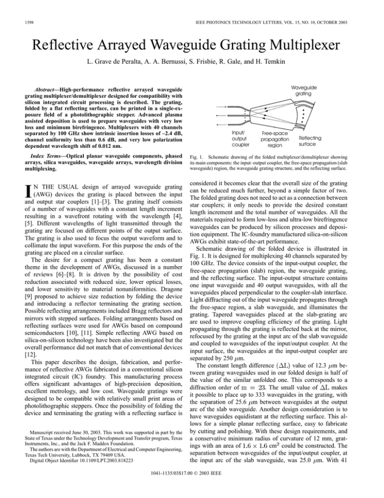
1398 IEEE PHOTONICS TECHNOLOGY LETTERS, VOL. 15, NO. 10, OCTOBER 2003 Reflective Arrayed Waveguide Grating Multiplexer L. Grave de Peralta, A. A. Bernussi, S. Frisbie, R. Gale, and H. Temkin Abstract—High-performance reflective arrayed waveguide grating multiplexer/demultiplexer designed for compatibility with silicon integrated circuit processing is described. The grating, folded by a flat reflecting surface, can be printed in a single-exposure field of a photolithographic stepper. Advanced plasma assisted deposition is used to prepare waveguides with very low loss and minimum birefringence. Multiplexers with 40 channels separated by 100 GHz show intrinsic insertion losses of –2.4 dB, channel uniformity less than 0.6 dB, and very low polarization dependent wavelength shift of 0.012 nm. Index Terms—Optical planar waveguide components, phased arrays, silica waveguides, waveguide arrays, wavelength division multiplexing. I N THE USUAL design of arrayed waveguide grating (AWG) devices the grating is placed between the input and output star couplers [1]–[3]. The grating itself consists of a number of waveguides with a constant length increment resulting in a wavefront rotating with the wavelength [4], [5]. Different wavelengths of light transmitted through the grating are focused on different points of the output surface. The grating is also used to focus the output waveform and to collimate the input waveform. For this purpose the ends of the grating are placed on a circular surface. The desire for a compact grating has been a constant theme in the development of AWGs, discussed in a number of reviews [6]–[8]. It is driven by the possibility of cost reduction associated with reduced size, lower optical losses, and lower sensitivity to material nonuniformities. Dragone [9] proposed to achieve size reduction by folding the device and introducing a reflector terminating the grating section. Possible reflecting arrangements included Bragg reflectors and mirrors with stepped surfaces. Folding arrangements based on reflecting surfaces were used for AWGs based on compound semiconductors [10], [11]. Simple reflecting AWG based on silica-on-silicon technology have been also investigated but the overall performance did not match that of conventional devices [12]. This paper describes the design, fabrication, and performance of reflective AWGs fabricated in a conventional silicon integrated circuit (IC) foundry. This manufacturing process offers significant advantages of high-precision deposition, excellent metrology, and low cost. Waveguide gratings were designed to be compatible with relatively small print areas of photolithographic steppers. Once the possibility of folding the device and terminating the grating with a reflecting surface is Manuscript received June 30, 2003. This work was supported in part by the State of Texas under the Technology Development and Transfer program, Texas Instruments, Inc., and the Jack F. Maddox Foundation. The authors are with the Department of Electrical and Computer Engineering, Texas Tech University, Lubbock, TX 79409 USA. Digital Object Identifier 10.1109/LPT.2003.818223 Fig. 1. Schematic drawing of the folded multiplexer/demultiplexer showing its main components: the input–output coupler, the free-space propagation (slab waveguide) region, the waveguide grating structure, and the reflecting surface. considered it becomes clear that the overall size of the grating can be reduced much further, beyond a simple factor of two. The folded grating does not need to act as a connection between star couplers; it only needs to provide the desired constant length increment and the total number of waveguides. All the materials required to form low-loss and ultra-low birefringence waveguides can be produced by silicon processes and deposition equipment. The IC-foundry manufactured silica-on-silicon AWGs exhibit state-of-the-art performance. Schematic drawing of the folded device is illustrated in Fig. 1. It is designed for multiplexing 40 channels separated by 100 GHz. The device consists of the input-output coupler, the free-space propagation (slab) region, the waveguide grating, and the reflecting surface. The input-output structure contains one input waveguide and 40 output waveguides, with all the waveguides placed perpendicular to the coupler-slab interface. Light diffracting out of the input waveguide propagates through the free-space region, a slab waveguide, and illuminates the grating. Tapered waveguides placed at the slab-grating arc are used to improve coupling efficiency of the grating. Light propagating through the grating is reflected back at the mirror, refocused by the grating at the input arc of the slab waveguide and coupled to waveguides of the input/output coupler. At the input surface, the waveguides at the input-output coupler are separated by 250 m. value of 12.3 m beThe constant length difference tween grating waveguides used in our folded design is half of the value of the similar unfolded one. This corresponds to a . The small value of makes diffraction order of it possible to place up to 333 waveguides in the grating, with the separation of 25.6 m between waveguides at the output arc of the slab waveguide. Another design consideration is to have waveguides equidistant at the reflecting surface. This allows for a simple planar reflecting surface, easy to fabricate by cutting and polishing. With these design requirements, and a conservative minimum radius of curvature of 12 mm, gratcm could be constructed. The ings with an area of separation between waveguides of the input/output coupler, at the input arc of the slab waveguide, was 25.0 m. With 41 1041-1135/03$17.00 © 2003 IEEE GRAVE DE PERALTA et al.: REFLECTIVE ARRAYED WAVEGUIDE GRATING MULTIPLEXER waveguides, one of which was used as the input, the entire coucm in area. pler was easily designed to be less than As a result, the grating and the input/output coupler fit convecm exposure field of a stepper. The niently into a grating and input/output coupler were each formed on a different lithographic mask (reticule). These were exposed sequentially during fabrication. The separation between masks, defining the slab waveguide, was controlled by the translation stage of the stepper with the accuracy of 0.1 m. After wafer fabrication, AWGs were separated by dicing and the input/output couplers and the reflecting surface terminating the waveguide grating were diamond polished to assure easy coupling and flatness, respectively. Fiduciary marks placed at the end of the grating were used to define the reflecting surface. High reflectivity of the reflecting surface was assured by the deposition of a Cr–Au film. difference The waveguide relative refractive index and , @1.55 m) between ( the core and the cladding materials was 0.68%, a conventional silica-on-silicon index step [8]. The waveguides were 5- m thick and were etched to produce 5–6- m wide cores. Pedestal-type waveguides were also used to control birefringence, as discussed below. Using beam propagation method and the above waveguide parameters, single mode operation and propagation losses less than 0.02 dB/cm, for a radius of curvature of 12.0 mm, were simulated. Small footprint of the grating and input/output sections makes it possible to print it with lithographic steppers typical of silicon IC foundries. The remaining question is the compatibility of materials available in such foundries with optical devices. The deposited on waveguides of interest consist of layers of a silicon substrate. The lower cladding layer of undoped , m thick, is prepared by high-pressure thermal oxidation (HIPOX) of silicon. The equipment needed to produce it is available in many foundries where it is used to prepare field oxides. The core layer is doped with phosphorus (P) to increase the . The upper cladding layer, deindex over that of undoped posited over the patterned and etched core layer, has a thickness of 10–15 m and is typically doped with Boron (B) and P to have an index of refraction close to that of the lower cladding layer. The addition of boron lowers the softening temperature of the glass and modifies its reflow properties to provide complete coverage of the etched core layer. The primary method of deposition of silicon dioxide in IC manufacturing is now plasma assisted chemical vapor deposition (PECVD). It is capable of high deposition rates , and high incorat relatively low temperatures, 400–450 poration of dopants. PECVD deposition relies on reaction of tetraethylorthosilane (TEOS) and ammonia. The dopants, B and P, are derived from conventional sources of trimethylborate and trimethylphosphate, respectively. The core and top cladding used in this work were TEOS-based and delayers of posited by PECVD using commercial IC equipment (Applied Materials P5000) on 150-mm diameter silicon wafers. Depom/min were obtained at the susceptor sition rates of temperature of 430 . Low deposition temperature allowed us to prepare doped with 10% B and 3.5% P. High doping levels assure slight tensile stress in this material, needed to compensate compressive stress of the core. This combination of materials results in waveguides with very low birefringence 1399 Fig. 2. (a) Waveguide cross section and transmission response (two channels) at different polarizations (—:TE; —:TM) for devices fabricated (b) without and (c) with pedestal waveguide structure. [13]. Dopant calibration was based on X-ray fluorescence, infrared absorption, and optical reflectivity calibration tools available in the foundry. After deposition layers were annealed for 30 min. Post-deposition index and thickness at 920 uniformity maps were obtained using automated reflectivity measurements. Additional index measurements at 1.55- m were done using a prism coupler. Wafers were free of cracks or bubbles. Photolithography was done using a Canon stepper with 0.5 m optical resolution. The IC deposition equipment is capable of producing layers with excellent thickness and index uniformity. Index maps of 225 points obtained on 150-mm diameter wafers at 632.8 nm show variation of less than 0.0008. Thickness uniformity was controlled to better than 1.5%, without any special calibration procedures. With high-quality deposition and metrology tools available at the silicon IC line we were able to reproducibly obtain baseline single-mode waveguide losses of less than 0.02 dB/cm. A cross section of a waveguide fabricated by the processes described here is illustrated in Fig. 2(a). The core layer of below and P-TEOS glass is surrounded by HIPOX BP-TEOS above. The top layer was planarized in a high temperature anneal. The etch process defining the core was to form a pedestal in the HIPOX layer. This extended is done in order to embed the core, as much as possible, in a BP-TEOS glass with the thermal expansion coefficient closely matching that of the silicon substrate. This results in more uniform biaxial strain and lower birefringence [13]. The device response to TE and TM polarized input for waveguides without the pedestal is shown in Fig. 2(b). With the use of highly doped glass the shift between the two polarizations is 0.15 nm. This is considerably smaller than the shift of 0.3 nm obtained with conventional glasses [13], [14]. With the use of a pedestal waveguide the shift is reduced to less than 0.012 nm, as shown in Fig. 2(c). This is a negligibly small value. The physical parameters of the reflective AWG were chosen using the model of Muñoz et al. [15] and the resulting calculated 1400 TABLE I CALCULATED AND MEASURED PARAMETERS OF A FOLDED AWG DEVICE IEEE PHOTONICS TECHNOLOGY LETTERS, VOL. 15, NO. 10, OCTOBER 2003 parameters demonstrate high quality of the reflecting surface folding the grating, both in terms of the overall flatness and local roughness. A direct comparison between the measured and calculated performance of the folded AWG can be found in Table 1. A good agreement between the measured and modeled characteristics of the reflective AWG is evident. In summary, we describe high-performance arrayed waveguide grating multiplexers designed to be manufactured in silicon IC foundries. The device is folded by the introduction of a reflecting surface in the grating region. This allows for the printing of the entire grating in a single exposure field of a stepper. Excellent device performance is attributed to careful design, advanced manufacturing techniques, and excellent materials and metrology developed for silicon IC manufacturing. The performance of a reflected AWG presented here is very competitive with equivalent conventional devices made with similar silica-on-silicon technology. ACKNOWLEDGMENT The authors would like to thank X-Fab Texas for their support and encouragement. Fig. 3. Wavelength response of a 40–channel folded multiplexer device (—:TE; —:TM). device performance is shown in Table I. The calculated characteristics are compatible with those expected in conventional 40-channel AWG based on silica-on-silicon technology with the index step of 0.68% [8], [16]. Two important parameters describing the AWGs performance are the loss and the loss nonuniformity. We selected a free frequency spectral range of 8.4 THz in order to achieve loss nonuniformity of 0.5 dB. With the use of tapered waveguides, 22.5- m wide, in the grating region losses of 2.3 dB were simulated. In order to obtain a 3 dB channel bandwidth of at least 0.4 nm, a slab waveguide radius of 5 cm was used together with tapered waveguides, 9.6 m in width, in the input/output coupler. With 333 waveguides in the grating, adjacent waveguide crosstalk of 33 dB was calculated. This choice of parameters is very conservative and further size reduction, without the resulting performance decrease, appears possible. The overall performance of a 40–channel reflective AWG is demonstrated in Fig. 3. The device was designed for Gaussian response with channel-to-channel separation of 100 GHz. We reproducibly achieve insertion losses as low as 2.8 dB, including the loss contribution of 0.4 dB due to the mode field mismatch between the optical fibers and the waveguides, and loss nonuniformity of less than 0.6 dB. In some devices, insertion losses as small as 2.1 dB are measured, resulting in the intrinsic loss of 1.7 dB. Individual channel was measured at the channel’s center wavelength. Very low polarization dependent wavelength shift (PDWS) of 0.012 nm was obtained with the use of high-B glass and careful tailoring of stress through the use of pedestal-type waveguides. This results in very low polarization dependent loss (PDL) of 0.02 dB. We also achieve very low adjacent channel crosstalk of less than 30 dB which we attributed to excellent stepper photolithography [17]. These 2 REFERENCES [1] C. Dragone, “An N N optical multiplexer using a planar arangement of two star couplers,” IEEE Photon. Technol. Lett., vol. 3, pp. 241–243, 1991. [2] , “Optical Multiplexer/Demultiplexer,” U.S. patent 5 002 350, Mar. 26, 1991. [3] C. Dragone, C. A. Edwards, and R. C. Kistler, “Integrated optics N N multiplexer on silicon,” IEEE Photon. Technol. Lett., vol. 3, pp. 896–899, 1991. [4] M. Smit, “New focusing and dispersive planar component based on an optical phased array,” Electron. Lett., vol. 24, pp. 385–386, 1988. [5] H. Takahashi, S. Suzuki, K. Kato, and I. Nishi, “Arrayed waveguide grating for wavelength division multi/demultiplexer with nanometer resolution,” Electron. Lett., vol. 26, pp. 87–88, 1990. [6] C. K. Madsen and J. H. Zhao, Optical Filter Design and Analysis. New York: Wiley, 1999. [7] Y. P.Yuan P. Li and C. H.Charles H. Henry, Silicon optical bench waveguide technology, in Optical Fiber Telecommunications, vol. IIIB, ch. 8. [8] K.Katsunari Okamoto, Fundamentals of Optical Waveguides. New York: Academic, 2000, ch. 9, pp. 341–385. [9] C. Dragone, “Efficient Reflective Multiplexer Arrangement,” U.S. patent 5 450 511, Sept. 12, 1995. [10] M. Zirngibl, “Waveguide Grating Router and Method of Making Same Having Relatively Small Dimensions,” U.S. patent 5 745 616, Apr. 28, 1998. [11] J. B. D. Soole, M. R. Amersfoort, H. P. LeBlanc, A. Rajhel, C. Caneau, C. Youtsey, and I. Adesida, “Compact polarization independent InP reflective arrayed waveguide grating filter,” Electron. Lett., vol. 32, pp. 1769–1771, 1996. [12] Y. Inoue, A. Himeno, K. Moriwaki, and M. Kawachi, “Silica-based arrayed-wave-guide grating circuit as optical splitter router,” Electron. Lett., vol. 31, pp. 726–727, Apr. 1995. [13] L. Grave de Peralta, A. A. Bernussi, H. Temkin, M. Borhani, and D. Doucette, “Silicon dioxide waveguides with low birefringence,” IEEE J. Quantum Electron., vol. 39, pp. 874–879, July 2003. [14] C. K. Nadler, E. K. Wildermuth, M. Lanker, W. Hunziker, and H. Melchior, “Polarization insensitive, low-loss, low-crosstalk wavelength multiplexer modules,” IEEE J. Select. Topics Quantum Electron., vol. 5, pp. 1407–1412, Sept./Oct. 1999. [15] P. Muñoz, D. Pastor, and J. Capmany, “Modeling and design of arrayed waveguide gratings,” J. Lightwave Technol., vol. 20, pp. 661–674, Apr. 2002. [16] A. Himeno, K. Kato, and T. Miya, “Silica-based planar lightwave circuits,” IEEE Select. Topics Quantum Electron., vol. 4, pp. 913–924, Nov.–Dec. 1998. [17] C. D. Lee, W. Chen, Q. Wang, Y. J. Chen, W. T. Beard, D. Stone, R. F. Smith, R. Mincher, and I. R. Stewar, “The role of photomask resolution on the performance of arrayed-waveguide grating devices,” J. Lightwave Technol., vol. 19, p. 1726, Nov. 2001. 2
