Table of Contents 1. Microscopy 1
advertisement
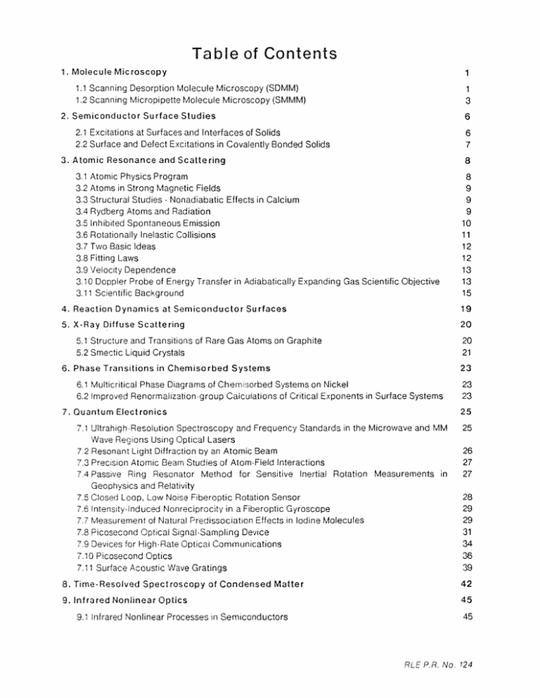
Table of Contents 1. Molecule Microscopy 1 1.1 Scanning Desorption Molecule Microscopy (SDMM) 1.2 Scanning Micropipette Molecule Microscopy (SMMM) 1 3 2. Semiconductor Surface Studies 6 2.1 Excitations at Surfaces and Interfaces of Solids 2.2 Surface and Defect Excitations in Covalently Bonded Solids 6 7 3. Atomic Resonance and Scattering 8 3.1 Atomic Physics Program 3.2 Atoms in Strong Magnetic Fields 3.3 Structural Studies - Nonadiabatic Effects in Calcium 3.4 Rydberg Atoms and Radiation 3.5 Inhibited Spontaneous Emission 3.6 Rotationally Inelastic Collisions 3.7 Two Basic Ideas 3.8 Fitting Laws 3.9 Velocity Dependence 3.10 Doppler Probe of Energy Transfer in Adiabatically Expanding Gas Scientific Objective 3.11 Scientific Background 8 9 9 9 10 11 12 12 13 13 15 4. Reaction Dynamics at Semiconductor Surfaces 19 5. X-Ray Diffuse Scattering 20 20 21 5.1 Structure and Transitions of Rare Gas Atoms on Graphite 5.2 Smectic Liquid Crystals 23 6. Phase Transitions in Chemisorbed Systems 6.1 Multicritical Phase Diagrams of Chemisorbed Systems on Nickel 6.2 Improved Renormalization-group Calculations of Critical Exponents in Surface Systems 23 23 25 7. Quantum Electronics 7.1 Ultrahigh-Resolution Spectroscopy and Frequency Standards in the Microwave and MM Wave Regions Using Optical Lasers 7.2 Resonant Light Diffraction by an Atomic Beam 7.3 Precision Atomic Beam Studies of Atom-Field Interactions 7.4 Passive Ring Resonator Method for Sensitive Inertial Rotation Measurements in Geophysics and Relativity 7.5 Closed Loop, Low Noise Fiberoptic Rotation Sensor 7.6 Intensity-induced Nonreciprocity in a Fiberoptic Gyroscope 7.7 Measurement of Natural Predissociation Effects in Iodine Molecules 7.8 Picosecond Optical Signal-Sampling Device 7.9 Devices for High-Rate Optical Communications 7,.10 Picosecond Optics 7.11 Surface Acoustic Wave Gratings 25 26 27 27 28 29 29 31 34 36 39 8. Time-Resolved Spectroscopy of Condensed Matter 42 9. Infrared Nonlinear Optics 45 9.1 infrared Nonlinear Processes in Semiconductors 45 RLE P.R. No. 124 10. Quantum Optics and Electronics 10.1 Nonlinear Optical Interactions in Semiconductors 10.2 Picosecond Dye Laser Optics 10.3 Nonlinear Spectroscopy of Atoms and Molecules 11. Microwave and Millimeter Wave Techniques 11.1 Research Objectives 12. Microwave and Quantum Magnetics 12.1 Tutorial Review of MSW 12.2 Magnetostatic Modes Bound by DC Field Gradients 12.3 Optical and Inductive Probing of Magnetostatic Resonances 12.4 Mode Synthesis 12.5 New Techniques to Guide and Control Magnetostatic Waves 12.6 Magnetostatic Wave Dispersion Theory 12.7 Velocity of Energy Circulation of Magnetostatic Modes 12.8 Magnetoelastic Waves and Devices 12.9 Short Millimeter Wave Magnetics 13. Radio Astronomy 13.1 Microwave Spectroscopy of the Interstellar Medium 13.2 Research Objectives 13.3 Long-Baseline Astrometric Interferometer 13.4 Controlled Thin-Film Antenna 13.5 Improved Microwave Retrieval Techniques 13.6 Communications Satellites 13.7 Video-Bandwidth Compression Techniques 13.8 Scanning Multichannel Microwave Radiometer (SMMR) 13.9 Tiros-N Satellite Microwave Sounder 13.10 Advanced Microwave Sounding Unit 13.11 Jovian Decametric Radiation 14. Electromagnetic Wave Theory and Remote Sensing 14.1 Electromagnetic Waves 14.2 Remote Sensing with Electromagnetic Waves 14.3 Acoustic Wave Propagation Studies 14.4 Effect of Earth Terrain on Millimeter Wave Propagation 14.5 Theories for Microwave Remote Sensing of Snow 14.6 SAR Image Prediction, Simulation, and Analysis 14.7 Remote Sensing of Vegetation and Soil Moisture 47 47 48 48 51 51 53 55 61 63 65 67 69 70 71 72 73 73 74 75 76 76 77 78 78 79 80 81 82 82 82 83 83 83 84 84 15. Electronic Properties of Amorphous Silicon Dioxide 87 16. Photon Correlation Spectroscopy and Applications 90 16.1 Research Program 17. Submicron Structures Fabrication and Research 17.1 Submicron Structures Fabrication 17.2 Submicron-Period Gold Transmission Gratings for Soft X-ray Spectroscopy 17.3 Spatial-Period-Division 90 92 92 93 93 RLE P.R. No. 124 17.4 Fabrication of X-ray Masks Using Anisotropic Etching of (110) SI and Shadowing Techniques 17.5 Reactive Sputter Etching of Si, SiO 2 , Cr, and Al with Gas Mixtures Based on CF 4, Cl2, and SiCI 4 17.6 Studies of Graphoepitaxy by CVD and Solution Growth 17.7 Graphoepitaxy for Solar Cells 17.8 Liquid Phase Epitaxy of InP 17.9 Filters Based on the Coupling of Surface Acoustic Waves in Gratings to Bulk Plate Modes 17.10 Fabrication of Corrugated-Gate MOS Structures 17.11 Narrow Inversion Layers in Silicon 17.12 Collaborative Projects 18. Plasma Dynamics 18.1 18.2 18.3 18.4 18.5 18.6 Relativistic Electron Beams and Generation of Coherent Electromagnetic Radiation Nonlinear Wave Interactions - RF Heating and Current Generation in Plasmas Tokamak Research: RF Heating and Current Drive Physics of Thermonuclear Plasmas Tokamak Research: RF Heating and Current Drive Preparation of Ozone 96 97 98 99 99 100 101 105 112 118 121 124 125 127 Improved Low-Visibility Optical Communication Atmospheric Propagation Effects on Infrared Radars Improved Millimeter-Wave Communication Through Rain Fiber-Coupled External-Cavity Semiconductor High-Power Laser 127 129 131 133 20. Digital Signal Processing 20.1 20.2 20.3 20.4 20.5 95 105 19. Optical Propagation and Communication 19.1 19.2 19.3 19.4 94 137 Introduction The Parabolic Wave Equation Knowledge-Based Signal Processing MEM Spectral Estimation for Non-uniformly Sampled Signals Geophysical Inversion by Velocity Spectra Migration and Joint Travel-time and Amplitude Techniques 20.6 A Comparison of Power Spectrum Estimation Techniques for Array Data 20.7 Characterization of a Atherosclerosis Using Pulse Doppler Ultrasound 20.8 Pole-Zero Modelling and Classification of Phonocardiograms 20.9 Reflection Coefficient Estimation in the Borehole Environment 20.10 One and Two Dimensional Maximum Entropy Spectral Estimation 20.11 Investigation of the Importance of Phase of the Residual Error Signal in the Linear Predictive Model of Speech 20.12 The Determination of the Acoustic Reflection Coefficient of the Ocean Bottom from its Response to a Point Source 20.13 Optimal Signal Reconstruction and ARMA Model Identification Given Noisy and Incomplete Observation Data 20.14 Artificial Intelligence and Signal Processing in Scene Analysis 20.15 Signal Reconstruction from the Short-Time Fourier Transform Magnitude 20.16 MEM Power Spectral Estimation with Uncertainty in Correlation Measurements 20.17 Unimportance of Phase in Speech 20.18 Comparison of Fast Hankel Transforms 137 139 140 140 141 142 143 144 144 145 145 146 146 147 148 148 148 149 RLE P.R. No. 124 21. Speech Communication 150 22. Linguistics 152 23. Cognitive Information Processing 154 154 23.1 Picture Coding 23.2 Digital Wirephoto 20 System 23.3 Graphic Arts Applications 23.4 Graphics Processing for Yearbook Production 23.5 Automated Engraving of Gravure Printing 156 157 158 159 24. Custom Integrated Circuits 159 162 24.1 Conversidn of Algorithms to Custom Integrated Circuits 24.2 VERY LARGE-SCALE INTEGRATED CIRCUIT RESEARCH 164 25. Communications Biophysics 25.1 Basic and Clinical Studies of the Auditory System 25.2 Middle Ear 25.3 Inner Ear Transduction 25.4 Coding in the Cochlear Nerve 25.5 Central Nervous System 25.6 Intensity Perception and Loudness 25.7 Hearing Aid Research 25.8 Tactile Communication of Speech 25.9 Acoustic Emissions from Human Ears 25.10 Investigation of the Mechanical Basis of Frequency Selectivity and Tonotopic Organization in the Cochlea of the Alligator Lizard 26. Neurophysiology 26.1 Studies of Optical Properties of Biological Materials 27. Publications and Reports 27.1 Meeting Papers Presented 27.2 Journal Papers Published 27.3 Journal Papers Accepted for Publication 27.4 Letters to the Editor Published 27.5 Letters to the Editor Accepted for Publication 27.6 Special Publications 27.7 Technical Reports Published 164 164 165 165 166 167 169 174 177 179 182 182 185 185 201 211 213 215 215 216 28. Personnel 217 29. Research Support Index 226 RLE P.R. No. 124 List of Figures Figure 1-1: Figure Figure Figure Figure Figure Figure Figure Figure Figure Figure Figure Sequential view of reversible uncoupling experiment. (a) Interference contrast view (40X water-immersion objective) of apical surface of Necturus gall bladder before impalement. (b) Epifluorescent view of injected cell in uncoupled epithelium (80% CO2, 32 mM bicarbonate buffer) 10 minutes after injection with the fluorescent dye, Lucifer Yellow. No dye spreading is visible. (c) Epifluorescent view of epithelium showing dye coupling after switching to air-saturated buffer. Scale bar, 10 im. 7-1: Interferometric sampler with strip-line resonator 7-2: Demultiplexer 7-3: Interferometer with 5-Waveguide "Y" 7-4: Schematic vies of the integrated XOR gate 12-1: Comparison between SAW and MSW normalized frequency dispersion. For a given wavelength X, the MSW frequency w2 can be much higher than the SAW frequency ~ . Moreover, since o(0) depends upon the dc bias, w is magnetically tunable. 12-2: Equivalent arithmetic operations provided by various analog signalprocessing devices. 12-3: Transverse section of a thin ferrite strip placed between ground planes. Longitudinal propagation of MSFVW, MSBVW, and MSSW results when, respectively, the dc bias is parallel to the X3 , X2 , X1 axis. 12-4: Normalized MSW frequency dispersion for the geometry of Figure 12.2 when the dc magnetic bias is oriented parallel to (a) x3' (b) x2 , and (c)x1 axis. The respective modes are termed MSFVW, MSBVW, and MSSW. 12-5: MSSW mode potentials of a finite slab for opposite directions of propagation. Localization occures near the surface for which the mode is more nearly positive-circularly polarized and is termed field-displacement nonreciprocity. The solid curve is for P out of the paper. 12-6: Geometry of curved-path experiment 12-7: Transmission characteristics of curved-path delay line Figure Figure Figure Figu re Figure Figure Figure 12-8: Probe tips of induction probe 12-9: Schematic of Induction Probe 12-10: Probe tip on LPE-YIG thin film 12-11: MSSW profiles 12-12: Schematic Diagram of microstrip transducer geometry 12-13: Experimental diplexer with YIG film removed 12-14: Diplexer Characteristics, Hdc = 1460 Oe a. Channel 1, MSSW b. Channel 2, MSBVW c. Composite Figure 17-1: Left: End view of PMMA exposed by x-ray lithography and developed. 0.3 tm period, 0.7 /m thick. Right: End view of gold grating. 0.3 /im period, 0.6 ,m thick. The gold was plated up between the PMMA grating lines shown in the top view and then the PMMA was dissolved away. Figure 17-2: Top view of PMMA x-ray exposed with crystallographic mask. The period of the grating is 0.3 m and the lines are smooth to + 4 nm. RLE P.R. No. 124 131 Figure 19-1: Scattered-to-Direct-Beam Power Ratio vs. Extinction Thickness 133 shown are components laser External-cavity Figure 19-2: Optical layout of experiments. in a top, cutaway view through the four-bar Super-Invar supporting structure. The labeled elements are: PM - plane mirror; SL - spherical collimating lens; D - diode gain element; CL - 40-mm diameter cylindrical lens; GL - graded-index (GRIN) rod lens; F - 14-cm-long optical fiber; P - polarizer; SM - spherical mirror. The polarizer was removed for some experiments. The plane mirror (PM) was replaced by a grating in the Littrow configuration in other experiments (the output in this case was the zero order of the grating). Figure 19-3: (a) Spectrum of stimulated emission output of external cavity containing 134 series combination of a diode gain element and a multimode fiber. (b) Fabry-Perot scan of this spectrum. Top trace shows entire 1500-MHz instrument resolution. These results are typical for output powers up to the 2-mW level set by diode life considerations. Figure 19-4: Concept of fiber-coupled external cavity semiconductor high-power laser 135 illustrating from left-to-right: the semiconductor-diode gain element whose left facet is coated for near-unity reflectivity and whose right facet is antireflection coated; electrooptic element for phase shifting; focusing lens; the appropriate spatial filter to assure coherence of wavefront across entire fiber bundle emitter (illustrated schematically as a stop); focusing lens to recollimate beam; and a partially reflecting mirror. The external cavity is bounded on the left by the reflecting facets of the semi-conductor gain elements and the right by the partially reflecting mirror. RLE P.R. No. 124
