Chapter 8. Novel Superconducting Tunneling Structures
advertisement
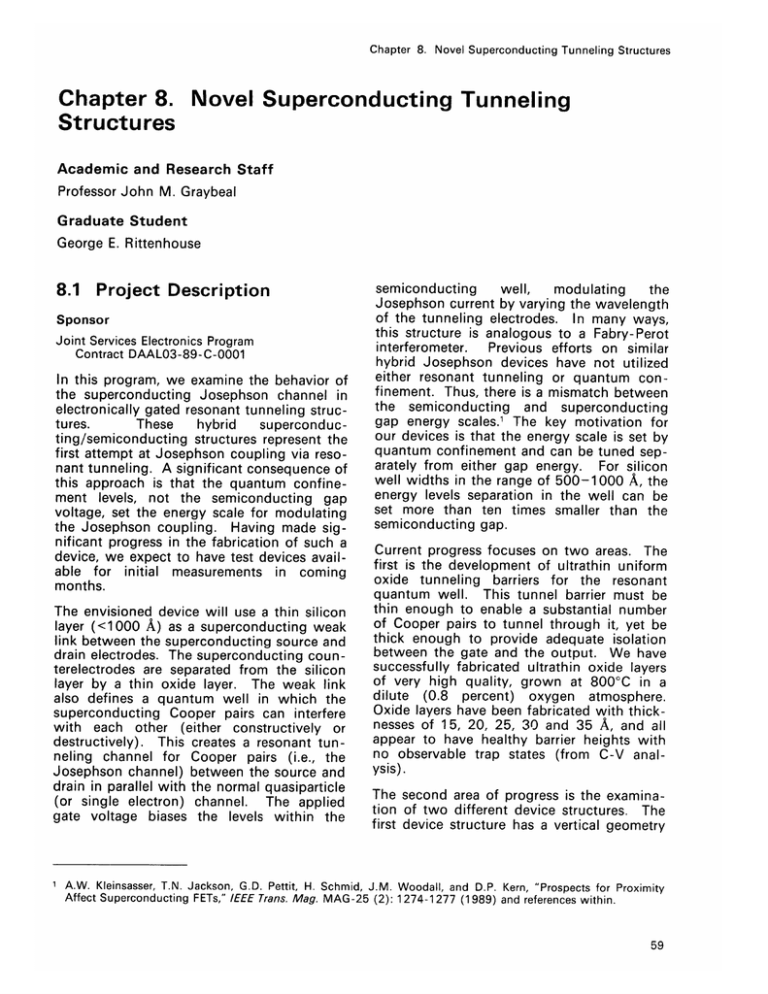
Chapter 8. Novel Superconducting Tunneling Structures Chapter 8. Novel Superconducting Tunneling Structures Academic and Research Staff Professor John M. Graybeal Graduate Student George E. Rittenhouse 8.1 Project Description Sponsor Joint Services Electronics Program Contract DAAL03-89-C-0001 In this program, we examine the behavior of the superconducting Josephson channel in electronically gated resonant tunneling structures. These hybrid superconducting/semiconducting structures represent the first attempt at Josephson coupling via resonant tunneling. A significant consequence of this approach is that the quantum confinement levels, not the semiconducting gap voltage, set the energy scale for modulating the Josephson coupling. Having made significant progress in the fabrication of such a device, we expect to have test devices available for initial measurements in coming months. The envisioned device will use a thin silicon layer (<1000 A) as a superconducting weak link between the superconducting source and drain electrodes. The superconducting counterelectrodes are separated from the silicon layer by a thin oxide layer. The weak link also defines a quantum well in which the superconducting Cooper pairs can interfere with each other (either constructively or destructively). This creates a resonant tunneling channel for Cooper pairs (i.e., the Josephson channel) between the source and drain in parallel with the normal quasiparticle (or single electron) channel. The applied gate voltage biases the levels within the semiconducting well, modulating the Josephson current by varying the wavelength of the tunneling electrodes. In many ways, this structure is analogous to a Fabry-Perot interferometer. Previous efforts on similar hybrid Josephson devices have not utilized either resonant tunneling or quantum confinement. Thus, there is a mismatch between the semiconducting and superconducting gap energy scales.' The key motivation for our devices is that the energy scale is set by quantum confinement and can be tuned separately from either gap energy. For silicon well widths in the range of 500-1000 A, the energy levels separation in the well can be set more than ten times smaller than the semiconducting gap. Current progress focuses on two areas. The first is the development of ultrathin uniform oxide tunneling barriers for the resonant quantum well. This tunnel barrier must be thin enough to enable a substantial number of Cooper pairs to tunnel through it, yet be thick enough to provide adequate isolation between the gate and the output. We have successfully fabricated ultrathin oxide layers of very high quality, grown at 8000 C in a dilute (0.8 percent) oxygen atmosphere. Oxide layers have been fabricated with thicknesses of 15, 20, 25, 30 and 35 A, and all appear to have healthy barrier heights with no observable trap states (from C-V analysis). The second area of progress is the examination of two different device structures. The first device structure has a vertical geometry 1 A.W. Kleinsasser, T.N. Jackson, G.D. Pettit, H. Schmid, J.M. Woodall, and D.P. Kern, "Prospects for Proximity Affect Superconducting FETs," IEEE Trans. Mag. MAG-25 (2): 1274-1277 (1989) and references within. Chapter 8. Novel Superconducting Tunneling Structures and uses a silicon membrane as the weak link, a geometry that has been fabricated before albeit for much thicker silicon membrane thicknesses. The second structure is a novel new structure, done in collaboration with Professor Henry I. Smith. This structure has a lateral geometry with a silicon wall as the weak link. Both are shown in figure 1. The operational physics of the two structures is identical. St. oIn starting material for this device is (100) Si. The wall is formed by a strongly anisotropic potassium-hydroxide wet etch. As this weak link is defined by a mask layer, no etch stop is necessary. Therefore, this fabrication route places no constraints on the dopant type or level in the wafer, which is very desirable. Also, the mechanical integrity of this device is substantially more robust. In addition, the lateral structure allows it to be more easily integrated into circuits. The primary difficulty in fabricating this lateral device is the production of the mask and the alignment of the mask pattern to the crystalline axes of the underlying wafer. We believe that both of these problems are surmountable, and our work is progressing on both fronts. Indeed, although we need to make some refinements, we have successfully produced thin silicon walls on test chips (figure 2). After finalizing the fabrication route, we will then begin careful measurement and analysis of the device behavior. Gate / Figure 1. (a) Vertical device geometry, and (b) lateral device geometry. Note: drawings are not to scale. In the vertical structure, the membrane is formed by an isotropic etch in ethylenediamine-pyrocatechol. This etch stops on a heavily boron-doped 1.75 /m thick layer deposited at the surface of the wafer. After this etch, the membrane is thinned to the desired thickness. Two disadvantages of this structure are its extreme fragility and its process limitation, being only heavily borondoped. The advantage of the structure is that its fabrication requires only one level of conventional VLSI optical lithography. However, we have found the fabrication of membranes much thinner than 1 ym to be exceedingly difficult, primarily due to fabrication-induced mechanical stresses. We have therefore stopped work on this particular structure. The second device structure has a lateral The topology, as shown in figure 1(b). 60 RLE Progress Report Number 132 Figure 2. Nanow (500A) wall structure (on right) etched into Si<110> wafer. Note scale at bottom of figure.
