Comparison of cross-talk effects between colloidal quantum dot and conventional waveguides
advertisement
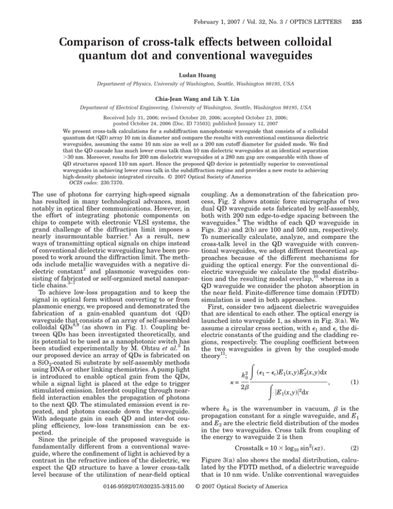
February 1, 2007 / Vol. 32, No. 3 / OPTICS LETTERS 235 Comparison of cross-talk effects between colloidal quantum dot and conventional waveguides Ludan Huang Department of Physics, University of Washington, Seattle, Washington 98195, USA Chia-Jean Wang and Lih Y. Lin Department of Electrical Engineering, University of Washington, Seattle, Washington 98195, USA Received July 31, 2006; revised October 20, 2006; accepted October 23, 2006; posted October 24, 2006 (Doc. ID 73503); published January 12, 2007 We present cross-talk calculations for a subdiffraction nanophotonic waveguide that consists of a colloidal quantum dot (QD) array 10 nm in diameter and compare the results with conventional continuous dielectric waveguides, assuming the same 10 nm size as well as a 200 nm cutoff diameter for guided mode. We find that the QD cascade has much lower cross talk than 10 nm dielectric waveguides at an identical separation ⬎30 nm. Moreover, results for 200 nm dielectric waveguides at a 280 nm gap are comparable with those of QD structures spaced 110 nm apart. Hence the proposed QD device is potentially superior to conventional waveguides in achieving lower cross talk in the subdiffraction regime and provides a new route to achieving high-density photonic integrated circuits. © 2007 Optical Society of America OCIS codes: 230.7370. The use of photons for carrying high-speed signals has resulted in many technological advances, most notably in optical fiber communications. However, in the effort of integrating photonic components on chips to compete with electronic VLSI systems, the grand challenge of the diffraction limit imposes a nearly insurmountable barrier.1 As a result, new ways of transmitting optical signals on chips instead of conventional dielectric waveguiding have been proposed to work around the diffraction limit. The methods include metallic waveguides with a negative dielectric constant2 and plasmonic waveguides consisting of fabricated or self-organized metal nanoparticle chains.3–7 To achieve low-loss propagation and to keep the signal in optical form without converting to or from plasmonic energy, we proposed and demonstrated the fabrication of a gain-enabled quantum dot (QD) waveguide that consists of an array of self-assembled colloidal QDs8,9 (as shown in Fig. 1). Coupling between QDs has been investigated theoretically, and its potential to be used as a nanophotonic switch has been studied experimentally by M. Ohtsu et al.5 In our proposed device an array of QDs is fabricated on a SiO2-coated Si substrate by self-assembly methods using DNA or other linking chemistries. A pump light is introduced to enable optical gain from the QDs, while a signal light is placed at the edge to trigger stimulated emission. Interdot coupling through nearfield interaction enables the propagation of photons to the next QD. The stimulated emission event is repeated, and photons cascade down the waveguide. With adequate gain in each QD and inter-dot coupling efficiency, low-loss transmission can be expected. Since the principle of the proposed waveguide is fundamentally different from a conventional waveguide, where the confinement of light is achieved by a contrast in the refractive indices of the dielectric, we expect the QD structure to have a lower cross-talk level because of the utilization of near-field optical 0146-9592/07/030235-3/$15.00 coupling. As a demonstration of the fabrication process, Fig. 2 shows atomic force micrographs of two dual QD waveguide sets fabricated by self-assembly, both with 200 nm edge-to-edge spacing between the waveguides.8 The widths of each QD waveguide in Figs. 2(a) and 2(b) are 100 and 500 nm, respectively. To numerically calculate, analyze, and compare the cross-talk level in the QD waveguide with conventional waveguides, we adopt different theoretical approaches because of the different mechanisms for guiding the optical energy. For the conventional dielectric waveguide we calculate the modal distribution and the resulting modal overlap,10 whereas in a QD waveguide we consider the photon absorption in the near field. Finite-difference time domain (FDTD) simulation is used in both approaches. First, consider two adjacent dielectric waveguides that are identical to each other. The optical energy is launched into waveguide 1, as shown in Fig. 3(a). We assume a circular cross section, with ⑀1 and ⑀c the dielectric constants of the guiding and the cladding regions, respectively. The coupling coefficient between the two waveguides is given by the coupled-mode theory11: = k02 2 冕 共⑀1 − ⑀c兲E1共x,y兲E2*共x,y兲dx 冕 , 共1兲 兩E1共x,y兲兩 dx 2 where k0 is the wavenumber in vacuum,  is the propagation constant for a single waveguide, and E1 and E2 are the electric field distribution of the modes in the two waveguides. Cross talk from coupling of the energy to waveguide 2 is then Crosstalk = 10 ⫻ log10 sin2共z兲. 共2兲 Figure 3(a) also shows the modal distribution, calculated by the FDTD method, of a dielectric waveguide that is 10 nm wide. Unlike conventional waveguides © 2007 Optical Society of America 236 OPTICS LETTERS / Vol. 32, No. 3 / February 1, 2007 Fig. 1. (Color online) Schematic drawing for the proposed QD waveguide.7 Fig. 2. (Color online) Atomic force micrograph images of QD waveguides. (a) 100 nm width, 200 nm edge-to-edge spacing dual QD waveguides; (b) 500 nm width, 200 nm edge-to-edge spacing dual QD waveguides. on a micrometer scale, the nanoscale waveguide appears to have the field distributed right outside the waveguide. When the waveguide diameter is increased to 200 nm, such a phenomenon disappears, and the guided mode shows a conventional modal distribution with the maximum centered in the waveguide. Now let us consider two identical adjacent QD waveguides, as shown in Fig. 3(b). An optical signal is sent into waveguide 1. The QD in the first waveguide will emit energy to its surroundings after stimulated emission, with the majority of the energy going in the propagation direction and absorbed by the next QD. The QD in the second waveguide will also absorb the energy that goes through its cross section, as shown in Fig. 3(c). Thus, the cross-talk level in the second QD waveguide can be characterized by considering the absorption process: = 冕 S · da 冒冕 S · dA, the dielectric waveguides and Poynting vector distribution for the QD waveguide shown in Figs. 3 and 4 are modeled by the FDTD method, where light with the wavelength at 633 nm and polarization in the y direction is used as the input signal. Figure 4 illustrates the modal distribution in the dielectric waveguides with different diameters. Note that in this work the size of QDs is the main factor affecting the simulation results. It affects the near-field Poynting vector distribution of the emitted light and energy coupling between the quantum dots. The quantized energy levels of QDs and resonant absorption have not been considered in the current model based on Eq. (3). The cross-talk level for all three waveguides is calculated by following the approaches previously described. For the QD waveguide, absorption by the adjacent QD with a 10 nm diameter is considered. For the dielectric waveguides, we calculated the energy coupling to the adjacent waveguide over a length of 10 nm. Figure 5 summarizes the simulation results, where 䊊 and 䊐 in the plot correspond to the case when two adjacent waveguides are spaced in the direction parallel to the polarization, which is along the y axis, while ⫹ and ⫻ represent the perpendicular orientation spaced in the x direction. The cross talk for these two situations is different, as the field distributions along x and y axes behave differently, as indicated by the curves in Fig. 4. For the 10 nm dielectric waveguide the field distribution for both directions reaches a maximum outside the waveguide core, and the distribution along the y axis decays faster than in the x direction, thus resulting in lower cross talk at larger separations. For a 200 nm dielectric waveguide, the field distribution shows that light is well confined in the x direction, while in the y direction there are side peaks outside the waveguide core with magnitudes similar to the central maximum, indicating that cross talk for waveguides spaced perpendicular to the polarization is lower. By convention, the simulation for the 200 nm waveguide starts from 200 nm center-to-center spacing, which is the smallest non-overlapping distance that can be modeled. 共3兲 where S is the Poynting vector, 兰da is the integration over the cross section of the QD in waveguide 2, and 兰dA is the integration over a whole sphere enclosing the emitting QD. Figure 3(b) also shows the Poynting vector distribution in the QD waveguide, as calculated by the FDTD method. In our model we simulated waveguides formed by 10 nm diameter QDs, which approximates the size of the core–shell nanoparticles used to fabricate the waveguides shown in Fig. 2 and lets the results be directly compared with a 10 nm dielectric waveguide. Furthermore, we examined the cross-talk effect for a 200 nm dielectric waveguide in which a conventional guided mode exists. The electric field distribution for Fig. 3. Schematic drawing showing the cross-talk effect in both waveguides (WG): (a) electric field distribution in conventional waveguides, (b) Poynting vector distribution in QD waveguides, (c) schematic showing calculation of cross talk in the QD waveguides. February 1, 2007 / Vol. 32, No. 3 / OPTICS LETTERS Fig. 4. Electric field distribution for dielectric waveguides with diameters of (a) 10, (b) 150, (c) 200, (d) 300 nm. The polarization of the light is along the y direction. 237 all, the simulation results suggest that the proposed QD waveguide can achieve a higher integration density, compared with conventional dielectric waveguides. In addition, the trend in Fig. 5 also shows that the QDs will have high energy coupling at very small separation, which suggests the feasibility of extremely flexible routing, such as 90° bends, as the optical energy can couple efficiently to the QD in a direction that is orthogonal to the propagation direction of the light. We have observed this effect experimentally.12 In this work, the cross talk level in a 10 nm colloidal quantum dot waveguide is calculated and compared with that of dielectric waveguides with 10 nm and 200 nm diameters. The simulation results show that the QD structure can achieve substantially lower cross talk compared with the dielectric waveguides. Therefore, the proposed device is a promising candidate for realizing high-density nanophotonic integrated circuits. We thank Babak A. Parviz for valuable discussions. C.-J. Wang thanks the National Science Foundation (NSF) Graduate Fellowship Program for financial support. The fabrication of the QD waveguide was performed in part at the University of Washington Nanotech User Facility (NTUF), a member of the National Nanotechnology Infrastructure Network (NNIN), which is supported by the NSF. Corresponding author L. Huang’s e-mail address is ldhuang@u.washington.edu. References Fig. 5. (Color online) Cross talk for the three waveguides over a distance of 10 nm. The horizontal axis represents the center-to-center distance between the waveguides. Comparing the cross talk in these three different waveguides, Fig. 5 shows that the cross talk in the QD waveguide is about 5 dB lower than that in the 10 nm dielectric waveguide at a separation distance of 30 nm. As expected, the difference increases with separation distance such that at a 100 nm gap the contrast in the transferred signal intensities is about 15 dB. The results show that cross talk for the 200 nm dielectric waveguide at a 280 nm separation is similar to that for the QD waveguide at a 110 nm separation. Looking at only conventional devices, cross talk in the 200 nm dielectric waveguide is comparable with that in the 10 nm dielectric waveguide at separations between 200 and 250 nm for the waveguide arrangement, as represented by the circles in Fig. 5. At larger spacings the 10 nm dielectric waveguide eventually has a higher cross talk due to the reduced confinement of the field distribution. Over- 1. C. M. Lieber, Sci. Am. 285, 58 (2001). 2. J. Takahara, S. Yamagishi, H. Taki, A. Morimoto, and T. Kobayashi, Opt. Lett. 22, 475 (1997). 3. M. L. Brongersma, J. W. Hartman, and H. A. Atwater, Phys. Rev. B 62, R16356 (2000). 4. S. A. Maier, P. G. Kik, H. A. Atwater, S. Meltzer, E. Harel, B. E. Koel, and A. A. G. Requicha, Nat. Mater. 2, 229 (2003). 5. M. Ohtsu, K. Kobayashi, T. Kawazoe, S. Sangu, T. Yatsui, IEEE J. Sel. Top. Quantum Electron. 8, 839 (2002). 6. M. Quinten, A. Leitner, J. R. Krenn, and F. R. Aussenegg, Opt. Lett. 23, 1331 (1998). 7. T. Yatsui, W. Nomura, and M. Ohtsu, Nano Lett. 5, 2548 (2005). 8. C.-J. Wang, L. Y. Lin, and B. A. Parviz, in Proceedings of IEEE LEOS 18th Annual Meeting (IEEE, 2005), pp. 177–178. 9. C.-J. Wang, L. Y. Lin, and B. A. Parviz, IEEE J. Sel. Top. Quantum Electron. 11, 500 (2005). 10. H. Kogelnik, in Guided-Wave Optoelectronics, 2nd ed., T. Tamir, ed. (Springer-Verlag, 1990), pp. 7–88. 11. L. A. Coldren and S. W. Corzine, Diode Lasers and Photonic Integrated Circuits (Wiley-Interscience, 1995). 12. C.-J. Wang, L. Huang, B. A. Parviz, and L. Y. Lin, Nano Lett. 6, 2549 (2006).
