Design of a Nanoelectromechanical High-Index-Contrast Guided-Wave Optical m
advertisement
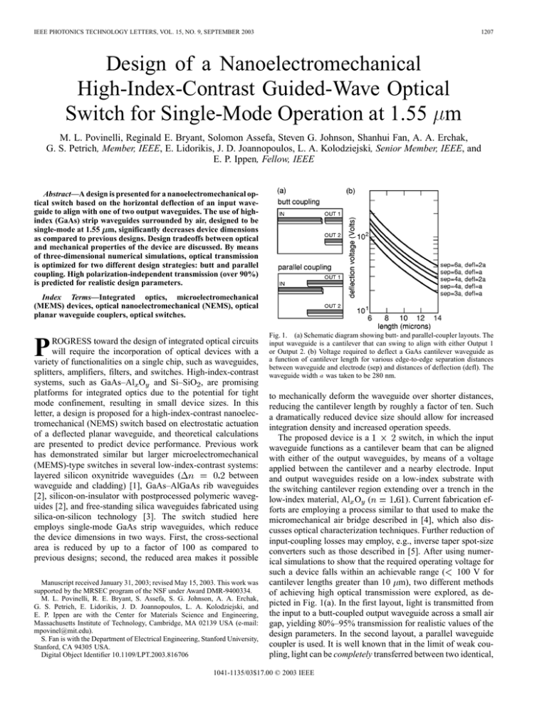
IEEE PHOTONICS TECHNOLOGY LETTERS, VOL. 15, NO. 9, SEPTEMBER 2003 1207 Design of a Nanoelectromechanical High-Index-Contrast Guided-Wave Optical Switch for Single-Mode Operation at 1.55 m M. L. Povinelli, Reginald E. Bryant, Solomon Assefa, Steven G. Johnson, Shanhui Fan, A. A. Erchak, G. S. Petrich, Member, IEEE, E. Lidorikis, J. D. Joannopoulos, L. A. Kolodziejski, Senior Member, IEEE, and E. P. Ippen, Fellow, IEEE Abstract—A design is presented for a nanoelectromechanical optical switch based on the horizontal deflection of an input waveguide to align with one of two output waveguides. The use of highindex (GaAs) strip waveguides surrounded by air, designed to be single-mode at 1.55 m, significantly decreases device dimensions as compared to previous designs. Design tradeoffs between optical and mechanical properties of the device are discussed. By means of three-dimensional numerical simulations, optical transmission is optimized for two different design strategies: butt and parallel coupling. High polarization-independent transmission (over 90%) is predicted for realistic design parameters. Index Terms—Integrated optics, microelectromechanical (MEMS) devices, optical nanoelectromechanical (NEMS), optical planar waveguide couplers, optical switches. P ROGRESS toward the design of integrated optical circuits will require the incorporation of optical devices with a variety of functionalities on a single chip, such as waveguides, splitters, amplifiers, filters, and switches. High-index-contrast systems, such as GaAs–Al O and Si–SiO , are promising platforms for integrated optics due to the potential for tight mode confinement, resulting in small device sizes. In this letter, a design is proposed for a high-index-contrast nanoelectromechanical (NEMS) switch based on electrostatic actuation of a deflected planar waveguide, and theoretical calculations are presented to predict device performance. Previous work has demonstrated similar but larger microelectromechanical (MEMS)-type switches in several low-index-contrast systems: between layered silicon oxynitride waveguides ( waveguide and cladding) [1], GaAs–AlGaAs rib waveguides [2], silicon-on-insulator with postprocessed polymeric waveguides [2], and free-standing silica waveguides fabricated using silica-on-silicon technology [3]. The switch studied here employs single-mode GaAs strip waveguides, which reduce the device dimensions in two ways. First, the cross-sectional area is reduced by up to a factor of 100 as compared to previous designs; second, the reduced area makes it possible Manuscript received January 31, 2003; revised May 15, 2003. This work was supported by the MRSEC program of the NSF under Award DMR-9400334. M. L. Povinelli, R. E. Bryant, S. Assefa, S. G. Johnson, A. A. Erchak, G. S. Petrich, E. Lidorikis, J. D. Joannopoulos, L. A. Kolodziejski, and E. P. Ippen are with the Center for Materials Science and Engineering, Massachusetts Institute of Technology, Cambridge, MA 02139 USA (e-mail: mpovinel@mit.edu). S. Fan is with the Department of Electrical Engineering, Stanford University, Stanford, CA 94305 USA. Digital Object Identifier 10.1109/LPT.2003.816706 Fig. 1. (a) Schematic diagram showing butt- and parallel-coupler layouts. The input waveguide is a cantilever that can swing to align with either Output 1 or Output 2. (b) Voltage required to deflect a GaAs cantilever waveguide as a function of cantilever length for various edge-to-edge separation distances between waveguide and electrode (sep) and distances of deflection (defl). The waveguide width a was taken to be 280 nm. to mechanically deform the waveguide over shorter distances, reducing the cantilever length by roughly a factor of ten. Such a dramatically reduced device size should allow for increased integration density and increased operation speeds. switch, in which the input The proposed device is a waveguide functions as a cantilever beam that can be aligned with either of the output waveguides, by means of a voltage applied between the cantilever and a nearby electrode. Input and output waveguides reside on a low-index substrate with the switching cantilever region extending over a trench in the ). Current fabrication eflow-index material, Al O ( forts are employing a process similar to that used to make the micromechanical air bridge described in [4], which also discusses optical characterization techniques. Further reduction of input-coupling losses may employ, e.g., inverse taper spot-size converters such as those described in [5]. After using numerical simulations to show that the required operating voltage for such a device falls within an achievable range ( 100 V for cantilever lengths greater than 10 m), two different methods of achieving high optical transmission were explored, as depicted in Fig. 1(a). In the first layout, light is transmitted from the input to a butt-coupled output waveguide across a small air gap, yielding 80%–95% transmission for realistic values of the design parameters. In the second layout, a parallel waveguide coupler is used. It is well known that in the limit of weak coupling, light can be completely transferred between two identical, 1041-1135/03$17.00 © 2003 IEEE 1208 Fig. 2. Transmission as a function of frequency for the butt-coupler device geometry, for = 11:3569 (GaAs). Units are given in terms of the waveguide width a. The gap between input and output waveguides was set to 0:32a (90 nm for a = 280 nm). The wavelength in micrometers for this choice of a is indicated on the top axis of the graph. parallel waveguides [6]. In this letter, it is demonstrated that a can be high, polarization-independent transmission of achieved in a high-index-contrast strongly coupled switch, as well as a single-polarization transmission of 98%. Further, a method for determining the optimal design parameters of such a device is presented. The operating voltage of the switch will depend on several device characteristics, including the dimensions of the cantilever beam, the waveguide-electrode separation, and the required deflection distance. Waveguides with a square cross section are used to allow for polarization independence. The waveguide width ( ) is chosen narrow enough to make the waveguide single mode at an operating wavelength of 1.55 m; in this case, nm. The separation distance between the cantilever waveguide and the (high-index) electrode should be large enough to – . The required demake optical coupling negligible, flection distance depends on the separation between the two output waveguides, which should be large enough to reduce the crosstalk to acceptable levels. A two-dimensional variational method was used to determine the static electromechanical response of the optical MEMS cantilever. A second-order differential equation describing the balance of Coulombic-induced electrostatic pressure and material elastic restoration pressure was iteratively solved within a prescribed error margin to determine the deformation of the cantilever during electrostatic distributed loading [7]. Fig. 1(b) shows the deflection voltage as a function of cantilever length for typical electrode-waveguide separations and deflection distances. The voltage decreases rapidly with cantilever length, falling, for example, within the readily achievable range of 20–40 V for a length of 14 m. Selection of an optimal cantilever length involves the balancing of several design considerations, since increasing the length will tend to both decrease the response time of the switch and increase the complexity of fabrication (due to stiction between the waveguide and the underlying substrate during the release process). The resonant frequency of the cantilever ranges from 1 MHz for a length of 15 m to 8 MHz for a length of 5 m. The switch is intended to operate well below the resonant frequency. The transmission was calculated for both designs using threedimensional (3-D) full-vectorial finite-difference time-domain (FDTD) simulations of Maxwell’s equations [8] with perfectly matched layer boundary regions [9]. Fig. 2 shows the trans- IEEE PHOTONICS TECHNOLOGY LETTERS, VOL. 15, NO. 9, SEPTEMBER 2003 mission as a function of frequency in the butt-coupled layout. The frequency is given in units of , where is the speed of light and is the waveguide width. Above the plot are shown the corresponding wavelengths in micrometers for a choice of nm. The width of the air gap was taken to be (90 nm), a conservative estimate of the experimentally achievable value. The transmission decreases as a function of increasing frequency (decreasing wavelength) and is identical for both polarizations, with a transmission of 80% at (1.55 m). (The two polarizations correspond to electromagnetic modes that are even (transverse electric-like) or odd (transverse magnetic (TM)-like) with respect to the horizontal midplane of the structure.) The reflection increases monotonically as a function of frequency from a value of 1% at a frequency of to 6% at . The remainder of the loss is due to radiation. For a fixed wavelength, the transmission can be increased by making the waveguide narrower, as can be seen from Fig. 2. Attention should be focussed on the lower axis (frequency) since the upper axis (wavelength) is only valid for a particular choice of . The transmission increases with decreasing , where is the dimensionless frequency given by . For a fixed physical wavelength , the corresponding value of is given by . Thus, for and m, for example, nm, and a transmission of 95% may be achieved for a nm. In practice, the choice of will ingap width of volve a tradeoff between the optical and mechanical properties of the cantilever beam and actual fabrication tolerances. Horizontal misalignment between input and output waveguides will , the reduce the transmission, e.g., for a displacement of over the frequency range reduction in transmission shown. An error in the waveguide width of 10 nm will result of . in a The parallel-coupler layout design provides an alternate means of increasing the transmission, without reducing the waveguide and/or air gap width. Fig. 3(a) shows the transmission as a function of frequency for a waveguide center-to-center separation of . The overlap distance of the two waveguides is set to , which is a near-optimal value for a separation of , as explained below. While the use of the waveguide coupler design introduces polarization dependence into the transmission spectrum, the two transmission curves cross , giving a polarization-independent transmission near of 92%. Moreover, the absolute difference in transmission between the two polarizations is less than 0.05 over a 50-nm . If preserving polarization bandwidth centered at independence is not essential, single-polarization transmission as high as 98% for the TM-like (odd) polarization can be – frequency range. achieved by operating in the The reflection was less than 2% for both polarizations in the entire frequency range shown, with significantly lower values at the optimal frequency for transmission. The optimal overlap length for a given separation can be estimated by means of a simple method, equivalent to first-order perturbation theory, that requires only the frequencies of the guided modes. It is assumed that the optimal overlap length is well approximated by the length required to completely transfer light between two infinitely long parallel waveguides. Coupling between the guides will split the original waveguide mode of and , frequency into states of frequencies POVINELLI et al.: DESIGN OF A NEMS HIGH-INDEX-CONTRAST GUIDED-WAVE OPTICAL SWITCH Fig. 3. (a) Transmission as a function of frequency for the parallel-coupler layout. The center-to-center separation of the waveguides is 2a and the overlap distance is 12a. The corresponding wavelength in micrometers is shown on the top axis for the choice a = 280 nm. (b) Optimum overlap length as a function of separation between the parallel waveguides. Filled and open symbols correspond to modes that are even and odd with respect to the mirror symmetry plane of the structure, respectively. corresponding to in-phase (symmetric) and out-of-phase (antisymmetric) combinations of the single-waveguide modes. If light is originally introduced into one waveguide, the time scale . To convert for transfer between the waveguides is to a length scale, is multiplied by the group velocity to get . is computed by applying a fully vectorial eigenmode solver [10] to find the modes of a parallel waveguide pair. From Fig. 3(b), it can be seen that the optimal overlap length increases exponentially as a function of waveguide separation, with the rate of increase dependent on the operating frequency. As the frequency increases, the modes become more localized in each waveguide, reducing their overlap and increasing the required length for transfer. If the input and output waveguides suffer a horizontal misalignment, the center-to-center separation is changed and the overlap length is no longer optimal. The severity of the effect is related to the slope of the graph in was the figure. From FDTD simulations, it was found that over the frequency range shown for a change in sepa. An error in the waveguide widths of 10 nm ration of results in a change in the transmission on the order of . The waveguide-coupling picture is also useful for estimating the crosstalk due to the coupling between the two output waveguides. (Scattering from the air gap between input and output waveguides will also contribute.) Given the center-to-center separation between the output waveguides, the crosstalk may , where is the coupling be estimated as is the overlap distance. Thus, for length of Fig. 3, and 1209 waveguides separated by (1.40 m) that run parallel to one (140 m) after the gap, , another for a distance of or 8 dB. The value of the crosstalk as calculated from 3-D FDTD simulations was less than 20 dB. In practice, even lower values of the crosstalk can be achieved by curving the output waveguides apart from one another away from the air trench region. To conclude, designs for an optical-NEMS switch based on the electrostatic actuation of GaAs waveguides surrounded by air have been presented. In contrast to previous work, high index contrast was used, reducing the dimensions of the switch and, hence, allowing for greater integration density. Two different physical mechanisms for achieving high transmission were discussed, butt coupling (with an air gap) and parallel-waveguide coupling. While the parallel-coupler design reduces reflection back into the input waveguide, the transmission is more sensitive to fabrication tolerances and misalignment. The relative merits of the two layouts are likely to be decided by experimental and fabrication considerations, as well as further study of the mechanical response of the switch. The butt and parallel-waveguide coupling mechanisms studied here should also be useful in the design of other integrated optoelectronic de(ON–OFF) switches with lower voltage requirevices, e.g., switch considered in this letter. ments than the ACKNOWLEDGMENT M. L. Povinelli would like to thank D. J. Ripin and P. Rakich for useful discussions, C. Luo for improvements to the FDTD code, and M. Watts for access to software. REFERENCES 2 [1] I. Shubin and P. L. K. Wa, “Electrostatically actuated 1 2 micromechanical optic switch,” Electron. Lett., vol. 37, pp. 451–452, Mar. 2001. [2] T. Bakke, C. P. Tigges, J. J. Lean, C. T. Sullivan, and O. B. Spahn, “Planar microoptomechanical waveguide switches,” IEEE J. Select. Topics Quantum Electron., vol. 8, pp. 64–71, Jan./Feb. 2002. [3] E. Ollier, “Optical MEMS devices based on moving waveguides,” IEEE J. Select. Topics Quantum Electron., vol. 8, pp. 155–162, Jan./Feb. 2002. [4] K.-Y. Lim, D. J. Ripin, G. S. Petrich, L. A. Kolodziejski, E. P. Ippen, M. Mondol, H. I. Smith, P. R. Villeneuve, S. Fan, and J. D. Joannopoulos, “Photonic band-gap waveguide microcavities: Monorails and air bridges,” J. Vac. Sci. Technol. B, vol. 17, pp. 1171–1174, May/June 1999. [5] T. Shoji, R. Tsuchizawa, T. Watanabe, K. Yamada, and H. Morita, “Spot-size converter for low-loss coupling between 0.3-m-square Si wire waveguides and single-mode fibers,” in Proc. LEOS Annu. Meeting, vol. 1, 2002, pp. 289–290. [6] B. E. A. Saleh and M. C. Teich, Fundamentals of Photonics. New York: Wiley, 1991, pp. 264–266. [7] P. M. Osterberg, “Electrostatically actuated microelectromechanical test structures for material property measurement,” Ph.D. dissertation, Massachusetts Inst. Technol., Cambridge, 1995. [8] K. S. Kunz and R. J. Luebbers, The Finite Difference Time Domain Method for Electromagnetics. Boca Raton, FL: CRC, 1993. [9] J. C. Chen and K. Li, “Quartic perfectly matched layers for dielectric waveguides and gratings,” Microwave Opt. Technol. Lett., vol. 10, pp. 319–323, Dec. 1995. [10] S. G. Johnson and J. D. Joannopoulos, “Block-iterative frequency-domain methods for Maxwell’s equations in a planewave basis,” Opt. Express, vol. 8, pp. 173–190, Jan. 2001.
