Document 10420986
advertisement

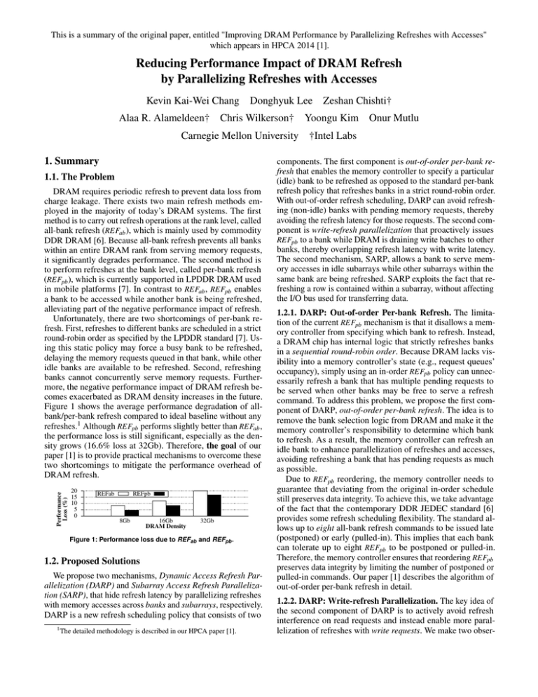
This is a summary of the original paper, entitled "Improving DRAM Performance by Parallelizing Refreshes with Accesses" which appears in HPCA 2014 [1]. Reducing Performance Impact of DRAM Refresh by Parallelizing Refreshes with Accesses Kevin Kai-Wei Chang Alaa R. Alameldeen† Donghyuk Lee Chris Wilkerson† Carnegie Mellon University 1. Summary 1.1. The Problem DRAM requires periodic refresh to prevent data loss from charge leakage. There exists two main refresh methods employed in the majority of today’s DRAM systems. The first method is to carry out refresh operations at the rank level, called all-bank refresh (REFab ), which is mainly used by commodity DDR DRAM [6]. Because all-bank refresh prevents all banks within an entire DRAM rank from serving memory requests, it significantly degrades performance. The second method is to perform refreshes at the bank level, called per-bank refresh (REFpb ), which is currently supported in LPDDR DRAM used in mobile platforms [7]. In contrast to REFab , REFpb enables a bank to be accessed while another bank is being refreshed, alleviating part of the negative performance impact of refresh. Unfortunately, there are two shortcomings of per-bank refresh. First, refreshes to different banks are scheduled in a strict round-robin order as specified by the LPDDR standard [7]. Using this static policy may force a busy bank to be refreshed, delaying the memory requests queued in that bank, while other idle banks are available to be refreshed. Second, refreshing banks cannot concurrently serve memory requests. Furthermore, the negative performance impact of DRAM refresh becomes exacerbated as DRAM density increases in the future. Figure 1 shows the average performance degradation of allbank/per-bank refresh compared to ideal baseline without any refreshes.1 Although REFpb performs slightly better than REFab , the performance loss is still significant, especially as the density grows (16.6% loss at 32Gb). Therefore, the goal of our paper [1] is to provide practical mechanisms to overcome these two shortcomings to mitigate the performance overhead of DRAM refresh. Performance Loss (%) 20 15 10 5 0 REFab REFpb 8Gb 16Gb DRAM Density 32Gb Figure 1: Performance loss due to REFab and REFpb . 1.2. Proposed Solutions We propose two mechanisms, Dynamic Access Refresh Parallelization (DARP) and Subarray Access Refresh Parallelization (SARP), that hide refresh latency by parallelizing refreshes with memory accesses across banks and subarrays, respectively. DARP is a new refresh scheduling policy that consists of two 1 The detailed methodology is described in our HPCA paper [1]. Zeshan Chishti† Yoongu Kim Onur Mutlu †Intel Labs components. The first component is out-of-order per-bank refresh that enables the memory controller to specify a particular (idle) bank to be refreshed as opposed to the standard per-bank refresh policy that refreshes banks in a strict round-robin order. With out-of-order refresh scheduling, DARP can avoid refreshing (non-idle) banks with pending memory requests, thereby avoiding the refresh latency for those requests. The second component is write-refresh parallelization that proactively issues REFpb to a bank while DRAM is draining write batches to other banks, thereby overlapping refresh latency with write latency. The second mechanism, SARP, allows a bank to serve memory accesses in idle subarrays while other subarrays within the same bank are being refreshed. SARP exploits the fact that refreshing a row is contained within a subarray, without affecting the I/O bus used for transferring data. 1.2.1. DARP: Out-of-order Per-bank Refresh. The limitation of the current REFpb mechanism is that it disallows a memory controller from specifying which bank to refresh. Instead, a DRAM chip has internal logic that strictly refreshes banks in a sequential round-robin order. Because DRAM lacks visibility into a memory controller’s state (e.g., request queues’ occupancy), simply using an in-order REFpb policy can unnecessarily refresh a bank that has multiple pending requests to be served when other banks may be free to serve a refresh command. To address this problem, we propose the first component of DARP, out-of-order per-bank refresh. The idea is to remove the bank selection logic from DRAM and make it the memory controller’s responsibility to determine which bank to refresh. As a result, the memory controller can refresh an idle bank to enhance parallelization of refreshes and accesses, avoiding refreshing a bank that has pending requests as much as possible. Due to REFpb reordering, the memory controller needs to guarantee that deviating from the original in-order schedule still preserves data integrity. To achieve this, we take advantage of the fact that the contemporary DDR JEDEC standard [6] provides some refresh scheduling flexibility. The standard allows up to eight all-bank refresh commands to be issued late (postponed) or early (pulled-in). This implies that each bank can tolerate up to eight REFpb to be postponed or pulled-in. Therefore, the memory controller ensures that reordering REFpb preserves data integrity by limiting the number of postponed or pulled-in commands. Our paper [1] describes the algorithm of out-of-order per-bank refresh in detail. 1.2.2. DARP: Write-refresh Parallelization. The key idea of the second component of DARP is to actively avoid refresh interference on read requests and instead enable more parallelization of refreshes with write requests. We make two obser- vations that lead to our idea. First, write batching in DRAM creates an opportunity to overlap a refresh operation with a sequence of writes, without interfering with reads. A modern memory controller typically buffers DRAM writes and drains them to DRAM in a batch to amortize the bus turnaround latency, also called tWTR or tRTW [6, 12, 13], which is the additional latency incurred from switching between serving writes to reads. Typical systems start draining writes when the write buffer occupancy exceeds a certain threshold until the buffer reaches a low watermark. This draining time period is called the writeback mode, during which no rank within the draining channel can serve read requests [2, 13, 20]. Second, DRAM writes are not latency-critical because processors do not stall to wait for them: DRAM writes are due to dirty cache line evictions from the last-level cache [13, 20]. Given that writes are not latency-critical and are drained in a batch for some time interval, they are more flexible to be scheduled with minimal performance impact. We propose the second component of DARP, write-refresh parallelization, that attempts to maximize parallelization of refreshes and writes. Write-refresh parallelization selects the bank with the minimum number of pending demand requests (both read and write) and preempts the bank’s writes with a per-bank refresh. As a result, the bank’s refresh operation is hidden by the writes in other banks. We refer the reader to Section 4 of our paper [1] for more details on the algorithm and implementation of DARP. Bank0 Subarray0 All-Bank or Per-Bank Refresh Time REFab/pb Subarray1 READ Time REF Delays Read Subarray Access Refresh Parallelization Bank0 Subarray0 REFab/pb Subarray1 READ Time Time Saved Cycles Figure 2: Service timeline of a refresh and a read request to two different subarrays within the same bank. Weighted Speedup 6 1.2.3. Subarray Access Refresh Parallelization (SARP). To tackle the problem of refreshes and accesses colliding within the same bank, we propose SARP (Subarray Access Refresh Parallelization) that exploits the existence of subarrays within a bank. The key observation leading to our second mechanism is that a refresh operation is constrained to only a few subarrays within a bank whereas the other subarrays and the I/O bus remain idle during the process of refreshing. The reasons for this are two-fold. First, refreshing a row requires only its subarray’s sense amplifiers that restore the charge in the row without transferring any data through the I/O bus. Second, each subarray has its own set of sense amplifiers that are not shared with other subarrays. Based on this observation, SARP’s key idea is to allow memory accesses to an idle subarray while other subarrays are refreshing. Figure 2 shows the service timeline and the performance benefit of our mechanism. As shown, SARP reduces the read latency by performing the read operation to Subarray 1 in parallel with the refresh in Subarray 0. Compared to DARP, SARP provides the following advantages: 1) SARP is applicable to both all-bank and per-bank refresh and 2) SARP enables memory accesses to a refreshing bank, which cannot be achieved with DARP. SARP requires modest modifications that reduce the sharing of the peripheral circuits for refreshes and accesses in each bank without changing the cell arrays. These modifications result in 0.71% DRAM die area overhead. Section 4.3 of our paper [1] describes these changes in detail. 7.9% 12.3% 20.2% 5 4 3 2 REFab REFpb DSARP No REF 1 0 8Gb 16Gb 32Gb DRAM Density 3.0% 5.2% 9.0% 45 40 35 30 25 20 15 10 5 0 8Gb 16Gb 32Gb DRAM Density Energy Per Access (nJ) ure 3 shows the average system performance and energy of our final mechanism, DSARP, the combination of DARP and SARP, compared to two baseline refresh schemes and an ideal scheme without any refreshes. The percentage numbers on top of the bars are the performance improvement of DSARP over REFab . We draw two observations. First, DSARP consistently improves system performance and energy efficiency over prior refresh schemes, capturing most of the benefit of the ideal baseline. Second, as DRAM density (refresh latency) increases, the performance benefit of DSARP gets larger. Figure 3: Average system performance and energy consumption. 2. Significance 2.1. Novelty To our knowledge, this is the first work to comprehensively study the effect of per-bank refresh and propose 1) a refresh scheduling policy built on top of per-bank refresh and 2) a mechanism that achieves parallelization of refresh and memory accesses within a refreshing bank. As a result, our mechanisms significantly improve system performance by effectively parallelizing refreshes with accesses. Prior works have investigated refresh scheduling policies on all-bank refresh or DDR4 fine granularity refresh to hide refresh operations behind rank idle time [17, 19].2 However, they provide minimal performance benefits because an all-bank refresh operates at the rank level, occupying all the banks, thus making it difficult to find a long enough idle period to hide the refresh latency. On the other hand, some works have proposed to exploit retention time variation among DRAM cells [15, 22]. Although this approach has the potential to reduce the number of refreshes, determining the retention time of DRAM cells accurately is still an unsolved research problem due to the Variable Retention Time and Data Pattern Dependence phenomena [11, 14]. In comparison, our proposed techniques 1.3. Summary of Results Here, we briefly summarize our results on an 8-core system. Section 6 of our paper provides the detailed evaluations. Fig- 2A recent work [21] that was published after our work proposes to operate DDR4 refresh at sub-rank level, which performs worse than per-bank refresh. 2 do not rely on retention time profiling and are guaranteed to preserve data integrity. Other works have proposed to skip refreshes in different scenarios. Ghosh and Lee [3] propose to skip refreshes to rows that had been recently accessed. Liu et al. [16] propose Flikker to lower refresh rate of non-critical data regions. Isen and John [5] propose ESKIMO to avoid refreshing invalid or unused data based on program semantics. DSARP is complementary to these techniques. (i.e., bank and subarray level) to mitigate worsening refresh overhead. Among many potential opportunities, one potential way to further reduce the refresh latency (i.e., tRFCab/pb ) is to trade off higher refresh rate (i.e., tREFI ), which is currently supported as fine granularity refresh in DDR4 DRAM for allbank refresh. In this work, we assume a fixed refresh rate for per-bank refresh as it is specified in the standard. Therefore, a new research question that our work raises is how can one combine per-bank refresh with fine granularity refresh and design a new scheduling policy for that? We think that DARP can inspire new scheduling policies to improve the performance of existing DRAM designs. 2.2. Potential Long Term Impact In this section, we describe three trends in the current and future DRAM subsystem that will likely make our proposed solutions more important in the future. References [1] K. K.-W. Chang et al., “Improving DRAM performance by parallelizing refreshes with accesses,” in HPCA, 2014. [2] N. Chatterjee et al., “Staged reads: Mitigating the impact of DRAM writes on DRAM reads,” in HPCA, 2012. [3] M. Ghosh and H.-H. S. Lee, “Smart Refresh: An Enhanced Memory Controller Design for Reducing Energy in Conventional and 3D Die-Stacked DRAMs,” in MICRO, 2007. [4] S. Hong, “Memory technology trend and future challenges,” in Intl. Electron Devices Meeting, 2010. [5] C. Isen and L. John, “Eskimo: Energy savings using semantic knowledge of inconsequential memory occupancy for dram subsystem,” in MICRO, 2009. [6] JEDEC, “DDR4 SDRAM Standard,” 2012. [7] JEDEC, “Low Power Double Data Rate 3 (LPDDR3),” 2012. [8] JEDEC, “High Bandwidth Memory (HBM) DRAM,” 2013. [9] JEDEC, “Low Power Double Data Rate 4 (LPDDR4),” 2014. [10] U. Kang et al., “Co-Architecting Controllers and DRAM to Enhance DRAM Process Scaling,” in The Memory Forum, 2014. [11] S. Khan et al., “The efficacy of error mitigation techniques for dram retention failures: A comparative experimental study,” in ACM SIGMETRICS, 2014. [12] Y. Kim et al., “A case for exploiting subarray-level parallelism (SALP) in DRAM,” in ISCA, 2012. [13] C. J. Lee et al., “DRAM-Aware last-level cache writeback: Reducing write-caused interference in memory systems,” in HPS Technical Report, 2010. [14] J. Liu et al., “An experimental study of data retention behavior in modern DRAM devices: Implications for retention time profiling mechanisms,” in ISCA, 2013. [15] J. Liu et al., “RAIDR: Retention-aware intelligent DRAM refresh,” in ISCA, 2012. [16] S. Liu et al., “Flikker: Saving dram refresh-power through critical data partitioning,” in Symp. on Architectural Support for Programming Languages and Operating Systems, 2011. [17] J. Mukundan et al., “Understanding and mitigating refresh overheads in high-density DDR4 DRAM systems,” in ISCA, 2013. [18] O. Mutlu, “Memory scaling: A systems architecture perspective,” in MemCon, 2013. [19] J. Stuecheli et al., “Elastic refresh: Techniques to mitigate refresh penalties in high density memory,” in MICRO, 2010. [20] J. Stuecheli et al., “The virtual write queue: Coordinating DRAM and last-level cache policies,” in ISCA, 2010. [21] V. K. Tavva et al., “Efgr: An enhanced fine granularity refresh feature for high-performance ddr4 dram devices,” TACO, vol. 11, no. 3, 2014. [22] R. Venkatesan et al., “Retention-aware placement in DRAM (RAPID): Software methods for quasi-non-volatile DRAM,” in HPCA, 2006. 2.2.1. Worsening retention time. As DRAM cells’ feature size continues to scale, the cells’ retention time will likely become shorter, exacerbating the refresh penalty [18]. When the surface area of cells gets smaller with further scaling, the depth/height of the cell needs to increase to maintain the same amount of capacitance that can be stored in a cell. In other words, the aspect ratio (the ratio of a cell’s depth to its diameter) needs to be increased to maintain the capacitance. However, many works have shown that fabricating high aspect-ratio cells is becoming more difficult due to processing technology [4, 10]. Therefore, cells’ capacitance (retention time) may potentially decrease with further scaling, increasing the refresh frequency. Using DSARP is a cost-effective way to alleviate the increasing negative impact of refresh as our results show [1]. 2.2.2. New DRAM standards with flexible per-bank refresh. According to the recently released DRAM standards, the industry is already in the process of implementing a similar concept of enabling the memory controller to determine which bank to refresh. In particular, the two standards are: 1) HBM [8] (October 2013, after the submission of our work) and 2) LPDDR4 [9] (August 2014). Both standards have incorporated a new refresh mode that allows per-bank refresh commands to be issued in any order by the memory controllers. Neither standard specifies a preferred order which the memory controller needs to follow for issuing refresh commands. Our work has done extensive evaluations to show that our proposed per-bank refresh scheduling policy, DARP, outperforms a naive round-robin policy by opportunistically refreshing idle banks. As a result, our policy can be potentially adopted in the future processors that use HBM or LPDDR4 DRAM. 2.2.3. Increasing number of subarrays. As DRAM density keeps increasing, more rows of cells are added within each DRAM bank. To avoid the disadvantage of increasing sensing latency due to longer bitlines in subarrays, more subarrays will likely be added within a single bank instead of increasing the size of each subarray. Our proposed refreshing scheme at the subarray level, SARP, becomes more effective at mitigating refresh as the number of subarrays increases because the probability of a refresh and a demand request colliding at the subarray level decreases with more subarrays. 2.3. New Research Directions This work will likely create new research opportunities for studying refresh scheduling policies at different dimensions 3


